Page History
...
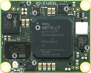
Trenz Electronic TE0712 is an industrial-grade FPGA module integrating a Xilinx Artix-7 FPGA, a 10/100 Mbit Ethernet transceiver, 1 GByte of DDR3 SDRAM, 32 MByte Flash memory for configuration and operation, and powerful switching-mode power supplies for all on-board voltages. Numerous configurable I/Os are provided via rugged high-speed strips. All this on a tiny footprint, smaller than a credit card size at very competitive price. All Trenz Electronic SoMs in 4 x 5 cm form factor are mechanically compatible.
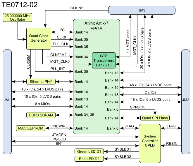
Block Diagram
Main Components
...
Programmable oscillator @25 MHz, SiTime SiT8008, U9
...
Programmable quad clock generator, Silicon Labs Si5338, U2
...
10/100 Mbps Ethernet PHY transceiver, Texas Instruments TLK106, U5
Key Features
- Xilinx Artix-7 FPGA
...
32 MByte QSPI Flash memory, Cypress S25FL256S, U4
...
4 Gbit DDR3 SDRAM, Intelligent Memory IM4G16D3EABG, U15
...
System Controller CPLD, Lattice Semiconductor MachXO2-256HC, U3
...
4 Gbit DDR3 SDRAM, Intelligent Memory IM4G16D3EABG, U19
...
Serial EEPROM, Microchip 11AA02E48, U7
...
- (15T to 200T) supported by the free Xilinx Vivado WebPACK software
- Both industrial and commercial temperature ranges available
- Rugged for high shock resistance and high vibration
- 1 GByte DDR3 32-bit SDRAM
- 10/100 Mbit Ethernet PHY
- MAC address EEPROM
- 32 MByte QSPI Flash memory (with XiP support)
- Programmable clock generator
- Transceiver clock (default 125 MHz)
- Fabric clock (default 200 MHz)
- Transceiver clock (default 125 MHz)
- Plug-on module with 2 × 100-pin and 1 × 60-pin high-speed hermaphroditic strips
- 158 FPGA I/Os (78 differential pairs) available via board-to-board connectors
- 4 GTP (high-performance transceiver) lanes
- GTP (high-performance transceiver) clock input
- On-board high-efficiency DC-DC converters
- 12A x 1.0V power rail
- 1.5A x 1.8V power rail
- 1.5A x 1.5V power rail
- System management and power sequencing
- eFUSE bit-stream encryption
- AES bit-stream encryption
- User configurable LEDs
- Evenly-spread supply pins for good signal integrity
Additional assembly options are available for cost or performance optimization upon request.
Block Diagram
Main Components
Programmable oscillator @25 MHz, SiTime SiT8008, U9
Programmable quad clock generator, Silicon Labs Si5338, U2
10/100 Mbps Ethernet PHY transceiver, Texas Instruments TLK106, U5
Xilinx Artix-7 FPGA XC7A series, U1
32 MByte QSPI Flash memory, Cypress S25FL256S, U4
4 Gbit DDR3 SDRAM, Intelligent Memory IM4G16D3EABG, U15
System Controller CPLD, Lattice Semiconductor MachXO2-256HC, U3
4 Gbit DDR3 SDRAM, Intelligent Memory IM4G16D3EABG, U19
Serial EEPROM, Microchip 11AA02E48, U7
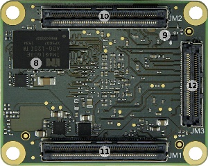
- Samtec Razor Beam™ LSHM-150 B2B connector, JM2
- Samtec Razor Beam™ LSHM-150 B2B connector, JM1
- Samtec Razor Beam™ LSHM-150 B2B connector, JM3
- 12A Enpirion EN63A0QI PowerSoC DC-DC converter, U14
- Green LED (SYSLED1), D1
- Red LED (SYSLED2), D2
Key Features
- Xilinx Artix-7 (15T to 200T) SoM (System on Module), supported by the free Xilinx Vivado WebPACK software
- Both industrial and commercial temperature ranges available
- Rugged for high shock resistance and high vibration
- 1 GByte DDR3 32-bit SDRAM
- 10/100 Mbit Ethernet PHY
- MAC address EEPROM
- 32 MByte QSPI Flash memory (with XiP support)
- Programmable clock generator
- Transceiver clock (default 125 MHz)
- Fabric clock (default 200 MHz)
- Transceiver clock (default 125 MHz)
- Plug-on module with 2 × 100-pin and 1 × 60-pin high-speed hermaphroditic strips
- 158 FPGA I/Os (78 differential pairs) available on board-to-board connectors
- 4 GTP (high-performance transceiver) lanes
- GTP (high-performance transceiver) clock input
- On-board high-efficiency DC-DC converters
- 12A x 1.0V power rail
- 1.5A x 1.8V power rail
- 1.5A x 1.5V power rail
- System management and power sequencing
- eFUSE bit-stream encryption
- AES bit-stream encryption
- User configurable LEDs
- Evenly-spread supply pins for good signal integrity
...
Initial Delivery State
Programmable unit | Content | Notes |
|---|---|---|
| Xilinx Artix-7 FPGA | Not programmed | U1 |
| System Controller CPLD | Programmed | U3 |
| SPI Flash OTP area | Empty | U4 |
SPI Flash main array | Empty | U4 |
| SPI Flash Quad Enable bit | Set | U4 |
Microchip 11AA02E48 | Globally unique EUI-48 (Ethernet MAC address) | U7 |
Signals, Interfaces and Pins
...
Special purpose pins are connected to System Controller CPLD and have following default configuration:
| Pin Name | Mode | Function | Default Configuration |
|---|---|---|---|
| PGOOD | Output | Power good | Active low when EN1 is low or module power is invalid. |
| JTAGEN | Input | JTAG select | Low for normal operation, high for System Controller CPLD access. |
| EN1 | Input | Power Enable | When forced low, pulls POR_B low to emulate power on reset. |
| NOSEQ | - | No function | Not used. |
| MODE | - | No function | Not used. |
Pin usages depends on CPLD Firmware, see: TE0712 CPLD
...
| LED | Color | SC Signal | SC Pin | Notes |
|---|---|---|---|---|
| D1 | Green | SYSLED1 | 9 | Exact function is defined by SC depends on System Controller CPLD firmware. |
| D2 | Red | SYSLED2 | 8 | Exact function is defined by SC depends on System Controller CPLD firmware. |
Clocking
Si5338 programmable clock generator is used to generate different clocks with 25 MHz oscillator connected to pin IN3. The Si5338 can alternatively be clocked using pins IN1 and IN2 which are connected to B2B connector JM3 (CLKIN2).
The Si5338 can be programmed to change the output frequency of the FPGA clocks (the Ethernet clock must remain at 50 MHz). An I2C I2C bus is connected between the FPGA (master) and clock generator (slave). Proper logic needs to be created in the FPGA to exercise the I2C I2C bus with the correct data. See the reference design section for more information.
...
Operating temperature range depends also on customer design and cooling solution. Please contact us for options.
Weight
21 16 - 27 g, Plain module (depends on variant).
8.8 g, Set of nuts and bolts.
Revision History
...
Date | Revision | Contributors | Description |
|---|---|---|---|
| 2017-03-01 | John Hartfiel | BUGFIX in the description of System Controller IO I/O section | |
| 2017-03-01 | v3.1 | John Hartfiel | Update Clocking Section |
| 2017-01-26 | V3 | Jan Kumann | New block diagram. Few corrections. |
| 2017-01-20 | V2
| Jan Kumann | Revised version. |
| 2013-12-02 | V0.1 | Antti Lukats | Work in progress. |
...
Overview
Content Tools