Page History
...
| Scroll Only (inline) |
|---|
Refer to https://shopwiki.trenz-electronic.de/dedisplay/Download/?path=Trenz_Electronic/TE0712PD/TE0712+TRM for downloadableonline version of this manual and the rest of available documentation. |
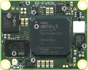
Trenz Electronic TE0712 is an industrial-grade FPGA module integrating a Xilinx Artix-7 FPGA, a 10/100 Mbit Ethernet transceiver, 1 GByte of DDR3 SDRAM, 32 MByte Flash memory for configuration and operation, and powerful switching-mode power supplies for all on-board voltages. Numerous configurable I/Os are provided via rugged high-speed strips. All this on a tiny footprint, smaller than a credit card size at very competitive price. All Trenz Electronic SoMs in 4 x 5 cm form factor are mechanically compatible.
...
Additional assembly options are available for cost or performance optimization upon request.
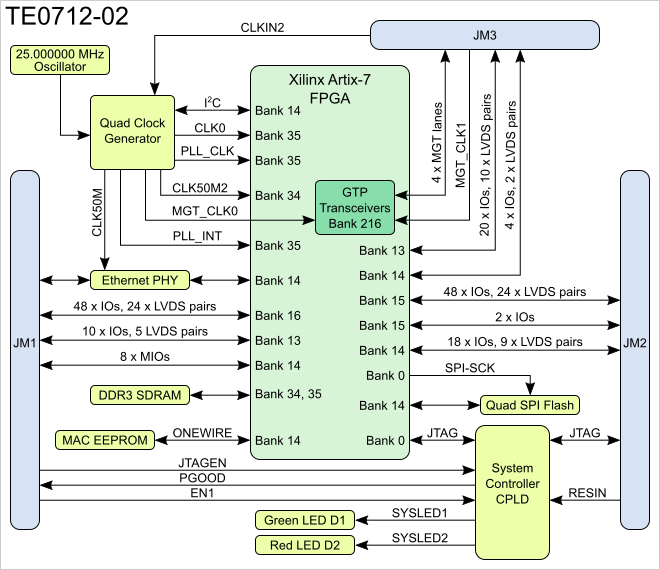
Block Diagram
| Page break |
|---|
Main Components
Programmable oscillator @25 MHz, SiTime SiT8008, U9
Programmable quad clock generator, Silicon Labs Si5338, U2
10/100 Mbps Ethernet PHY transceiver, Texas Instruments TLK106, U5
Xilinx Artix-7 FPGA XC7A series, U1
32 MByte QSPI Flash memory, Cypress S25FL256S, U4
4 Gbit DDR3 SDRAM, Intelligent Memory IM4G16D3EABG, U15
System Controller CPLD, Lattice Semiconductor MachXO2-256HC, U3
4 Gbit DDR3 SDRAM, Intelligent Memory IM4G16D3EABG, U19
Serial EEPROM, Microchip 11AA02E48, U7
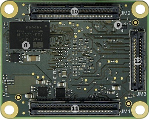
- Samtec Razor Beam™ LSHM-150 B2B connector, JM2
- Samtec Razor Beam™ LSHM-150 B2B connector, JM1
- Samtec Razor Beam™ LSHM-150 B2B connector, JM3
- 12A Enpirion EN63A0QI PowerSoC DC-DC converter, U14
- Green LED (SYSLED1), D1
- Red LED (SYSLED2), D2
...
FPGA bank number and number of I/O signals connected to the B2B connector:
| FPGA Bank | B2B Connector | I/O Signal Count | Voltage Level | Notes |
|---|---|---|---|---|
| 13 | JM1 | 10 | VCCIO13 | Supplied by the baseboard. |
| 13 | JM3 | 20 | VCCIO13 | Supplied by the baseboard. |
| 14 | JM1 | 8 | 3.3V | |
| 14 | JM2 | 18 | 3.3V | |
| 14 | JM3 | 4 | 3.3V | |
| 15 | JM2 | 48 | VCCIO15 | Supplied by the baseboard. |
| 15 | JM2 | 2 | VCCIO15 | Supplied by the baseboard. |
| 16 | JM1 | 48 | VCCIO16 | Supplied by the baseboard. |
Please refer to the Pin-out tables page for additional information.
...
| JTAGEN | JTAG Access To |
|---|---|
| Low | Artix-7 FPGA |
| High | System Controller CPLD |
| Page break |
|---|
System Controller I/O Pins
...
Pin usages depends on CPLD Firmware, see: TE0712 CPLD
On-board LEDs
The TE0712 module has 2 LEDs which are connected to the System Controller CPLD. Once FPGA configuration has completed these can be used by the user's design.
| LED | Color | SC Signal | SC Pin | Notes |
|---|---|---|---|---|
| D1 | Green | SYSLED1 | 9 | Exact function depends on System Controller CPLD firmware. |
| D2 | Red | SYSLED2 | 8 | Exact function depends on System Controller CPLD firmware. |
| Page break |
|---|
Clocking
Si5338 programmable clock generator is used to generate different clocks with 25 MHz oscillator connected to pin IN3. The Si5338 can alternatively be clocked using pins IN1 and IN2 which are connected to B2B connector JM3 (CLKIN2).
...
| CLK Output | FPGA Bank | FPGA Pin | IO Standard | Net Name | Default Frequency | Notes |
|---|---|---|---|---|---|---|
| CLK0* | 34 | K4/J4 | DIFF_SSTL15 | CLK0_P/N | -- | NB! Since PCB REV02. |
| CLK1A | - | - | CLK50M | 50 MHz | PHY chip RMII reference clock. | |
| CLK1B* | 34 | R4 | CLK50M2 | -- | NB! Since PCB REV02. | |
| CLK2 | 216 | F6/E6 | Auto | MGT_CLK0_P/N | 125 MHz | GTP transceiver clock. |
| CLK3 | 35 | H4/G4 | DIFF_SSTL15 | PLL_CLK_P/N | 50 MHz |
|
* See notes.
Board Connector Clock Inputs
Certain B2B connector pins are connected to the FPGA pins which are capable of handling clocking signals from the user’s PCB (baseboard). See schematics B2B page for additional information.
...
See Xilinx datasheet DS181 - "Artix-7 FPGAs Data Sheet: DC and AC Switching Characteristics" for additional information. User should also check related baseboard documentation when choosing baseboard design for TE0712 module.
| Page break |
|---|
Power Rails
Power Rail Name | B2B Connector JM1 Pin | B2B Connector JM2 Pin | Direction | Notes |
|---|---|---|---|---|
VIN | 1, 3, 5 | 2, 4, 6, 8 | Input | SoM supply voltage (from the baseboard). |
| 3.3VIN | 13, 15 | - | Input | SoM supply voltage (from the baseboard). |
| 1.5V | - | 19 | Output | Module internal 1.5V level. |
1.8V | 39 | - | Output | Module internal 1.8V level. Maximum 300mA available. |
| 3.3V | 14 | 10, 12 | Output | Module internal 3.3V level. |
| VCCIO13 | - | 1, 3 | Input | High-Range bank supply voltage (from the baseboard). |
| VCCIO15 | - | 7, 9 | Input | High-Range bank supply voltage (from the baseboard). |
| VCCIO16 | 9, 11 | - | Input | High-Range bank supply voltage (from the baseboard). |
| VREF_JTAG | - | 91 | Output | JTAG reference voltage (3.3V). |
...
| Include Page | ||||
|---|---|---|---|---|
|
Technical Specifications
...
Variants Currently In Production
Module Variant | FPGA | Junction Temperature | Temperature Range | B2B Connector Height |
|---|---|---|---|---|
| TE0712-02-35-2I | XC7A35T-2FGG484I | -40°C to 85°C | Industrial grade | 4.0 mm |
| TE0712-02-100-1I | XC7A100T-1FGG484I | -40°C to 85°C | Industrial grade | 4.0 mm |
| TE0712-02-200-1I | XC7A200T-1FBG484I | -40°C to 85°C | Industrial grade | 4.0 mm |
| TE0712-02-200-2I | XC7A200T-2FBG484I | -40°C to 85°C | Industrial grade | 4.0 mm |
| TE0712-02-200-1I3 | XC7A200T-1FBG484I | -40°C to 85°C | Industrial grade | 2.5 mm |
| TE0712-02-100-2C | XC7A100T-2FGG484C | 0°C to 85°C | Commercial grade | 4.0 mm |
| TE0712-02-100-2C3 | XC7A100T-2FGG484C | 0°C to 85°C | Commercial grade | 2.5 mm |
| TE0712-02-200-2C | XC7A200T-2FBG484C | 0°C to 85°C | Commercial grade | 4.0 mm |
| TE0712-02-200-2C3 | XC7A200T-2FBG484C | 0°C to 85°C | Commercial grade | 2.5 mm |
Technical Specifications
Absolute Maximum Ratings
Parameter | Min | Max | Units | Reference Document |
|---|---|---|---|---|
VIN supply voltage | -0.3 | 6.5 | V | EP53F8QI datasheet. |
| 3.3VIN supply voltage | -0.3 | 6.0 | V | TPS748 datasheet. |
| HR I/O banks supply voltage (VCCO) | -0.5 | 3.6 | V | Xilinx datasheet DS181 |
| HR I/O banks input voltage | -0.4 | VCCO + 0.55 | V | Xilinx datasheet DS181 |
| GTP transceivers Tx/Rx input voltage | -0.5 | 1.26 | V | Xilinx datasheet DS181 |
Storage temperature | -55 | 100 | °C | See IM4G16D3EABG datasheet. |
Recommended Operating Conditions
| Parameter | Min | Max | Units | Reference Document |
|---|---|---|---|---|
| VIN supply voltage |
| 2. |
| 4 |
| 5.5 | V |
| EP53F8QI datasheet. |
| 3.3VIN supply voltage |
| 2. |
| 9 |
| 5. |
| 5 | V | TPS748 datasheet. |
Storage temperature (ambient)
-55
100
°C
Recommended Operating Conditions
...
| HR I/O banks supply voltage (VCCO) | 1.14 | 3.465 | V | Xilinx datasheet DS181 |
| HR I/O banks input voltage | -0.20 | VCCO + 0.2 | V | Xilinx datasheet DS181 |
Operating Temperature Ranges
Commercial grade: 0°C to +70°C.
Industrial grade: -40°C to +85°C.
Operating temperature range depends also on customer design and cooling solution. Please contact us for options
...
.
| Note |
|---|
| Assembly variants for higher storage temperature range are available on request. |
| Page break |
|---|
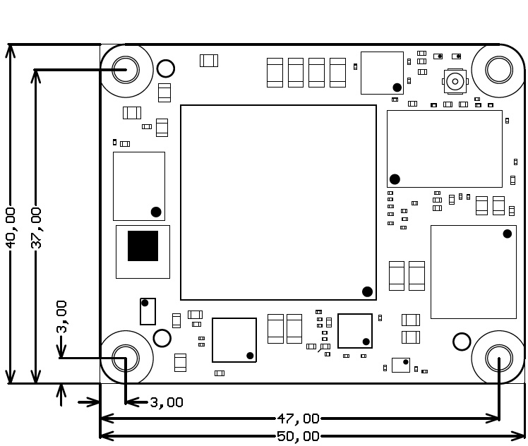
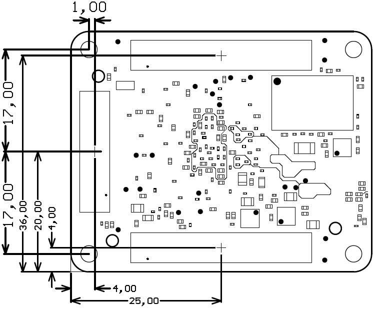
Physical Dimensions
- Module size: 50 mm × 40 mm. Please download the assembly diagram for exact numbers.
- Mating height with standard connectors: 8mm
- PCB thickness: 1.6mm
- Highest part on PCB: approx. 2.5mm. Please download the step model for exact numbers.
All dimensions are shown in millimeters.
Operating Temperature Ranges
Commercial grade: 0°C to +70°C.
Industrial grade: -40°C to +85°C.
Operating temperature range depends also on customer design and cooling solution. Please contact us for options.
- on PCB: approx. 2.5mm. Please download the step model for exact numbers.
All dimensions are shown in millimeters.
Weight
16 - 27 g, Plain module (depends on variant).
...
Hardware Revision History
| Date | Revision | Notes | PCN | Documentation Link |
|---|---|---|---|---|
| 2016-12-09 | 02 | Second production revision | Click to see PCN | TE0712-02 |
| 2013-12-02 | 01 | First production revision | TE0712-01 |
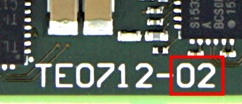
Hardware revision number is printed on the PCB board together with the module model number separated by the dash.
Document Change History
Date | Revision | Contributors | Description |
|---|---|---|---|
| 2017-05-29 | Jan Kumann | Variants table added. Key Features section relocated. | |
| 2017-03-01 | V3.2 | John Hartfiel | BUGFIX in the description of System Controller I/O section |
| 2017-03-01 | v3.1 | John Hartfiel | Update Clocking Section |
| 2017-01-26 | V3 | Jan Kumann | New block diagram. Few corrections. |
| 2017-01-20 | V2
| Jan Kumann | Revised version. |
| 2013-12-02 | V0.1 | Antti Lukats | Work in progress. |
Disclaimer
| Include Page | ||||
|---|---|---|---|---|
|
Overview
Content Tools