Page History
...
| Scroll Title | ||||||||||||||||||||||||||||||||||||||
|---|---|---|---|---|---|---|---|---|---|---|---|---|---|---|---|---|---|---|---|---|---|---|---|---|---|---|---|---|---|---|---|---|---|---|---|---|---|---|
| ||||||||||||||||||||||||||||||||||||||
|
...
- Plug the TE0835 module on the TEB0835 carrier board
- Install the cooler on the RFSoC chip
- Attention: It is strongly recommended that the RFSoC should not be used without heat sink.
- Connect the micro USB cable to the J29 connector
- Plug the board on the PCIe port of the PC
- Plug the prepared SD card on the SD card socket (J28)
- Connect a cable with SMA or UFL connector to one of the DAC connector( for example DAC0 J9) and feed it back to the related ADC input (for example ADC0 J1)
- (optional) A signal generator can be used to feed desired sinal to ADC input.
- (optional) An oscilloscope can be used to monitor the output signal of DAC.
...
| RF Analyzer GUI | Board TE0835 ( RFSoC U1) | TEB0835 | ||||
|---|---|---|---|---|---|---|
| Tile /Converter | SoC Pin Name | SoC Pin Number | B2B | Signal Name | Connector Designator | Connector Type |
| ADC Tile 0-ADC 01 | ADC0_P/ADC0_N | AK2/AK1 | B2B31/29 | ADC0_P/ADC0_N | J1 | SMA |
| ADC Tile 0-ADC 23 | ADC1_P/ADC1_N | AH2/AH1 | B2B43/41 | ADC1_P/ADC1_N | J2 | UFL |
| ADC Tile 1-ADC 01 | ADC2_P/ADC2_N | AF2/AF1 | B2B49/47 | ADC2_P/ADC2_N | J3 | SMA |
| ADC Tile 1-ADC 23 | ADC3_P/ADC3_N | AD2/AD1 | B2B59/61 | ADC3_P/ADC3_N | J4 | UFL |
| ADC Tile 2-ADC 01 | ADC4_P/ADC4_N | AB2/AB1 | B2B67/65 | ADC4_P/ADC4_N | J5 | SMA |
| ADC Tile 2-ADC 23 | ADC5_P/ADC5_N | Y2/Y1 | B2B79/77 | ADC5_P/ADC5_N | J6 | UFL |
| ADC Tile 3-ADC 01 | ADC6_P/ADC6_N | V2/V1 | B2B85/83 | ADC6_P/ADC6_N | J7 | SMA |
| ADC Tile 3-ADC 23 | ADC7_P/ADC7_N | T2/T1 | B2B97/95 | ADC7_P/ADC7_N | J8 | UFL |
| DAC Tile 0-DAC 0 | DAC0_P/DAC0_N | N2/N1 | B2B103/101 | DAC0_P/DAC0_N | J9 | SMA |
| DAC Tile 0-DAC 1 | DAC1_P/DAC1_N | L2/L1 | B2B109/107 | DAC1_P/DAC1_N | J10 | UFL |
| DAC Tile 0-DAC 2 | DAC2_P/DAC2_N | J2/J1 | B2B121/119 | DAC2_P/DAC2_N | J11 | SMA |
| DAC Tile 0-DAC 3 | DAC3_P/DAC3_N | G2/G1 | B2B127/125 | DAC3_P/DAC3_N | J12 | UFL |
| DAC Tile 1-DAC 0 | DAC4_P/DAC4_N | E2/E1 | B2B133/131 | DAC4_P/DAC4_N | J13 | UFL |
| DAC Tile 1-DAC 1 | DAC5_P/DAC5_N | C2/C1 | B2B139/137 | DAC5_P/DAC5_N | J14 | UFL |
| DAC Tile 1-DAC 2 | DAC6_P/DAC6_N | B4/A4 | B2B151/149 | DAC6_P/DAC6_N | J15 | UFL |
| DAC Tile 1-DAC 3 | DAC7_P/DAC7_N | B6/A6 | B2B157/155 | DAC7_P/DAC7_N | J16 | UFL |
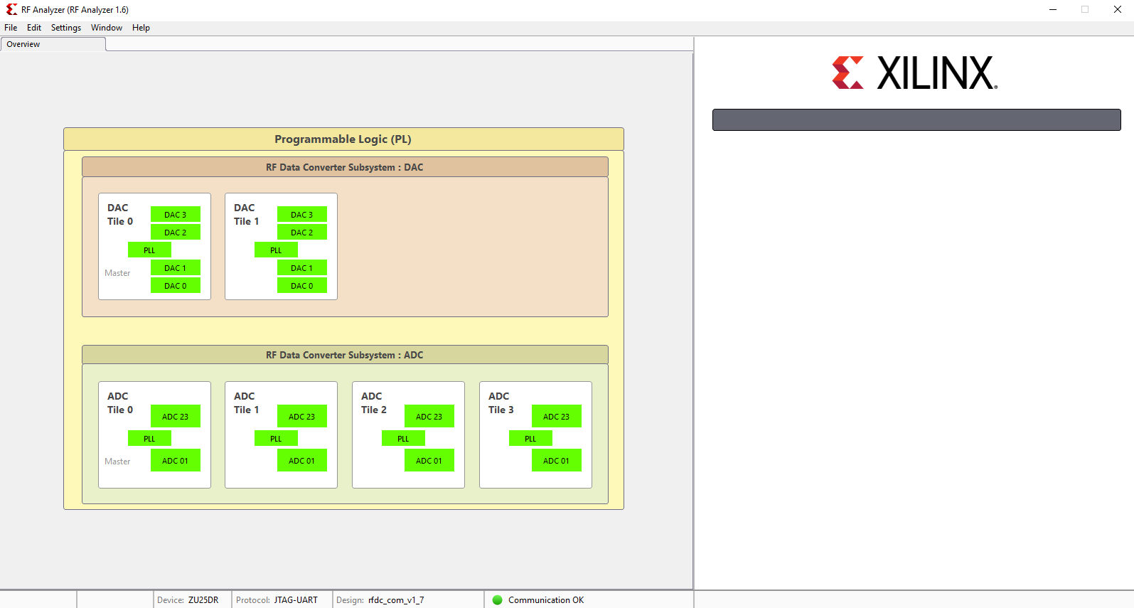
As an example the GUi should be seen after initialization as below:
| Expand | ||
|---|---|---|
| ||
|
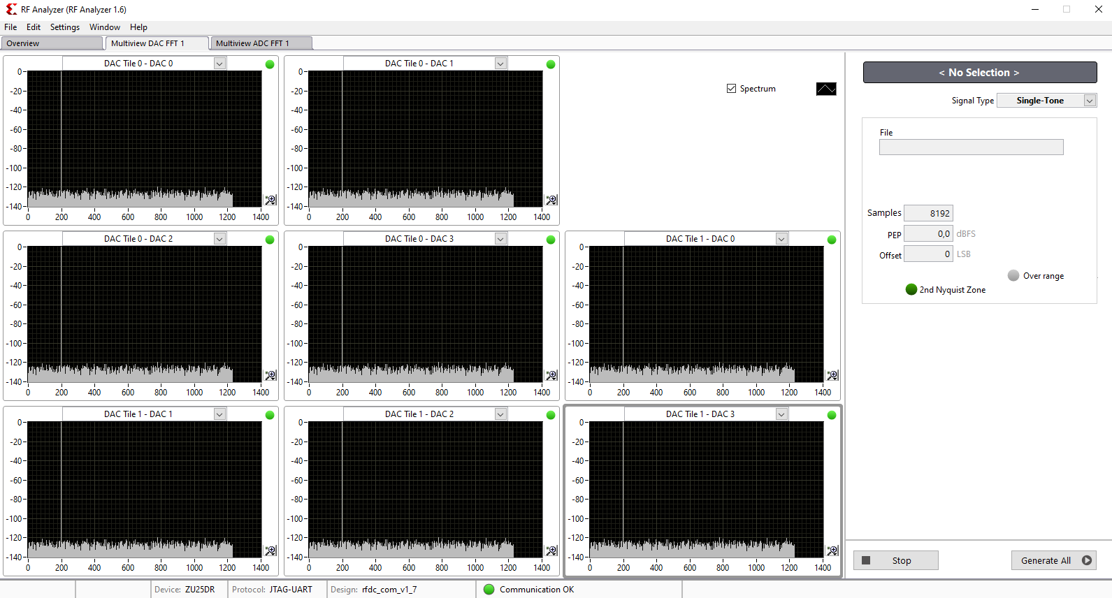
For example, when all DACs are in operation, the GUI can be seen as below:
| Expand | ||
|---|---|---|
| ||
|
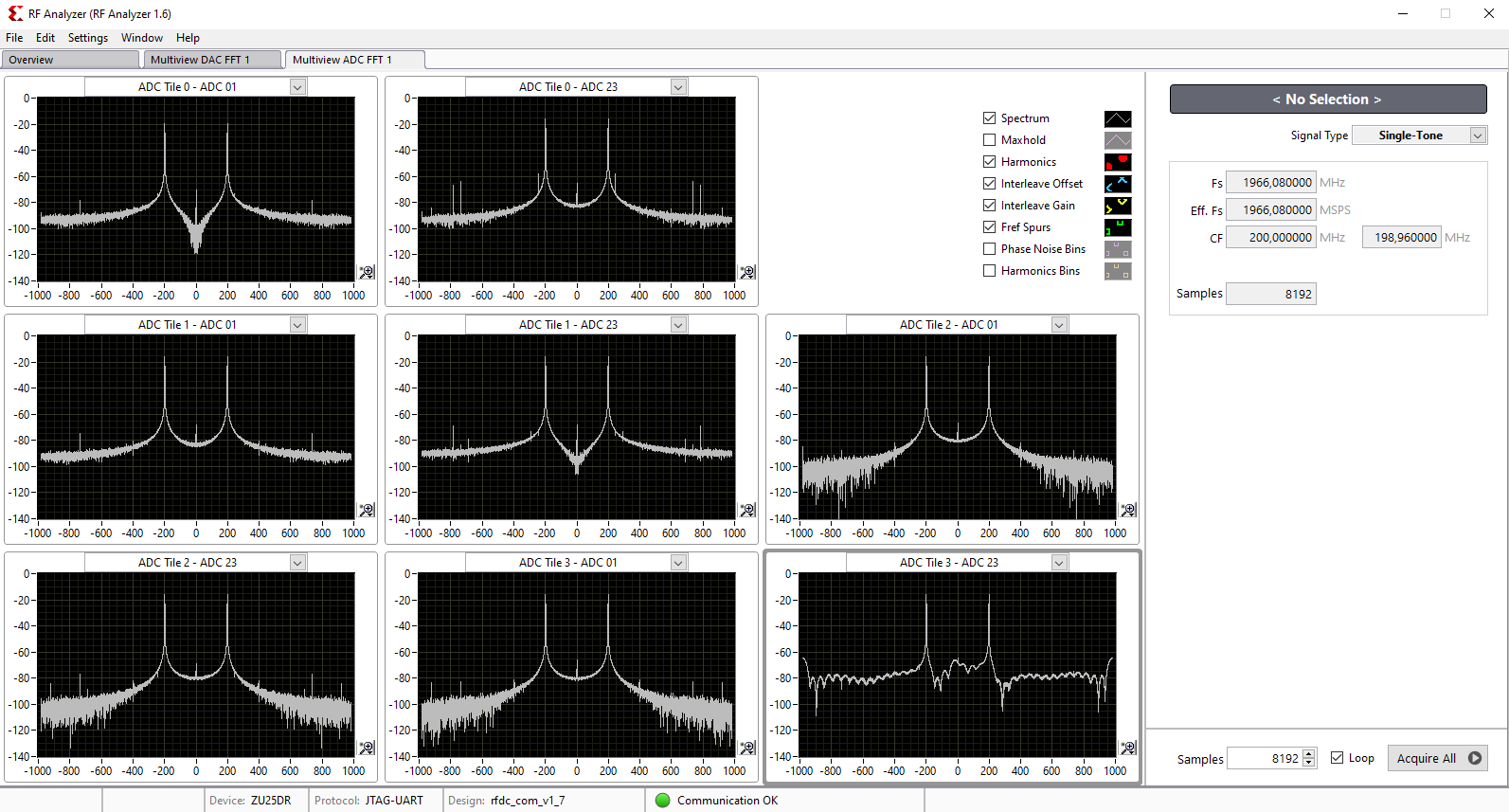
For example, when all ADCs are in operation, the GUI can be seen as below:
| Expand | ||
|---|---|---|
| ||
|
System Design - Vivado
...
Overview
Content Tools