| Page properties |
|---|
|
Template Revision 2.15
- Module: TRM Name always "TE Series Name" +TRM
Example: "TE0728 TRM" - Carrier: TRM Name usually "TEB Series Name" +TRM
Example: "TEB0728 TRM"
Template Change history: - 2.14 to 2.15
- add excerpt macro to key features
- 2.13 to 2.14
- add fix table of content
- add table size as macro
- 2.12 to 2.13
- Changed controller Signals section
|
| Page properties |
|---|
|
Important General Note:
|
| Page properties |
|---|
|
----------------------------------------------------------------------- |
| Page properties |
|---|
|
Note for Download Link of the Scroll ignore macro: |
Overview
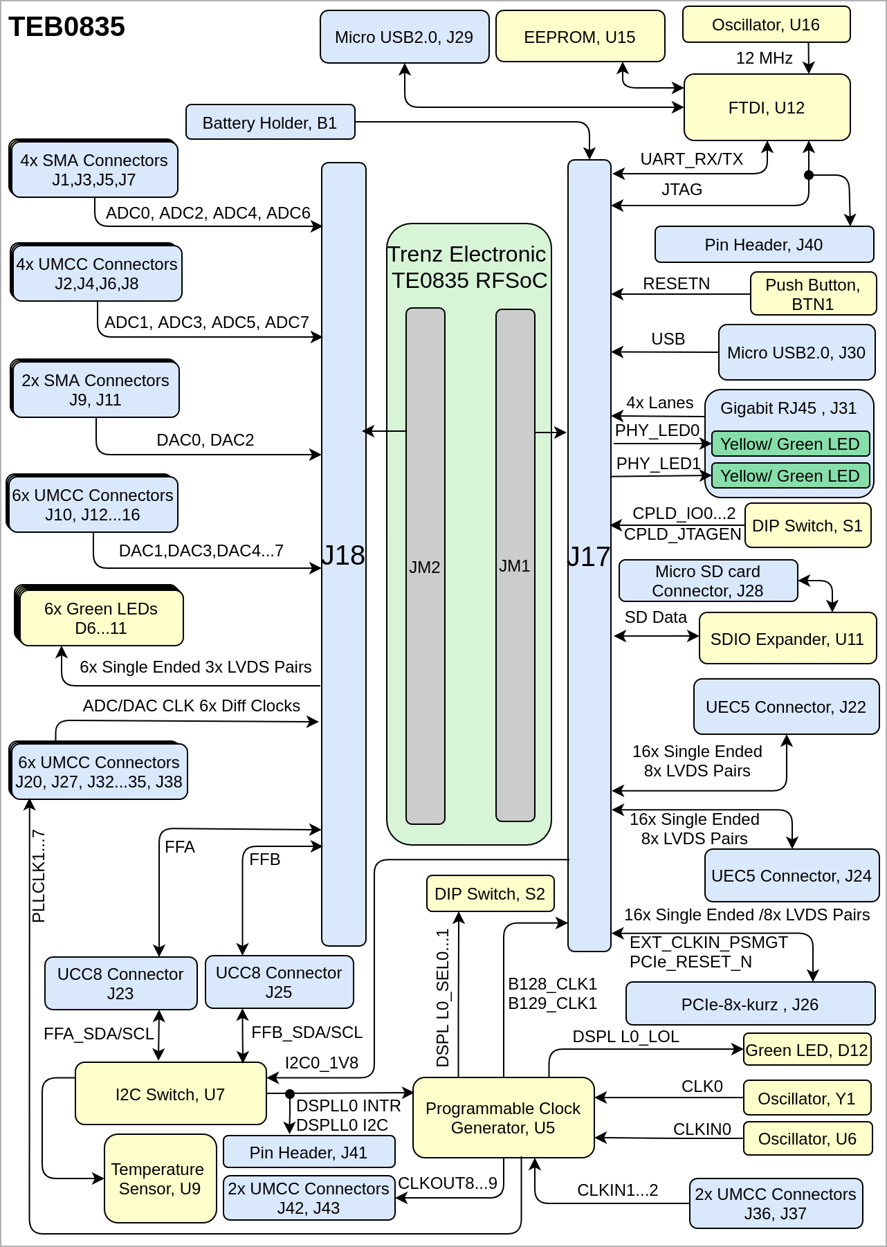
The Trenz Electronic TEB0835 is a carrier for TE0835 module which is based on Xilinx UltraScale+ RFSoC. The Carrier is equipped with a Micro SD card reader, Micro USB2.0, 21x UMCC connectors and 6x SMA connectors for clocks and ADC/DAC inputs/outputs , 6x Green User LEDs, Reset Push Button, DIP Switch for Mode, Battery Holder, FT2232H FTDI, programmable clock generators and a Temperature sensor IC. The carrier provides PCIe connector as well.
Refer to http://trenz.org/teb0835-info for the current online version of this manual and other available documentation.
Key Features
| Page properties |
|---|
|
Note:
'description: Important components and connector or other Features of the module
→ please sort and indicate assembly options Key Features' must be split into 6 main groups for modules and mainboards: - SoC/FPGA
- Package: SFVC784
- Device: ZU2...ZU5*
- Engine: CG, EG, EV*
- Speed: -1LI, -2LE,*, **
- Temperature: I, E,*, **
- RAM/Storage
- Low Power DDR4 on PS
- Data width: 32bit
- Size: def. 2GB*
- Speed:***
- eMMC
- Data width: 8Bit
- size: def. 8GB *
- QSPI boot Flash in dual parallel mode (size depends on assembly version)
- Data width: 8bit
- size: def. 128MB *
- HyperRAM/Flash (optional, default not assembled)
- MAC address serial EEPROM with EUI-48™ node identity (Microchip 24AA025E48)
- On Board
- Lattice LCMXO2
- PLL SI5338
- Gigabit Ethernet transceiver PHY (Marvell Alaska 88E1512)
- Hi-speed USB2 ULPI transceiver with full OTG support (Microchip USB3320C)
- Interface
- 132 x HP PL I/Os (3 banks)
- ETH
- USB
- 4 GTR (for USB3, Sata, PCIe, DP)
- MIO for UART
- MIO for SD
- MIO for PJTAG
- JTAG
- Ctrl
- Power
- 3.3V-5V Main Input
- 3.3V Controller Input
- Variable Bank IO Power Input
- Dimension
- Notes
- * depends on assembly version
- ** also non low power assembly options possible
- *** depends on used U+ Zynq and DDR4 combination
Key Features' must be split into 6 main groups for carrier: - Modules
- TE0808, TE807, TE0803,...
- RAM/Storage
- On Board
- Interface
- E.g. ETH, USB, B2B, Display port
- Power
- E.g. Input supply voltage
- Dimension
|
| Excerpt |
|---|
- Modules:
- RAM/Storage
- On Board
- Programmable Clock Generator
- I2C Switch IC
- 6x User Green LEDs
- 16x RF Transformation
- Reset Push Button
- Temperature Sensor
- FT2232H FTDI
- SDIO Port Expander
- 2x DIP Switch
- Pin Headers
- PCIe 6 Connector
- Interface
- 21x UMCC Connectors
- 6x SMA Connectors
- 2x Micro USB2.0
- RJ45 LAN Socket
- Micro SD Card Socket
- 2x UEC5 Connectors
- 2x UCC8 Connectors
- PCIe x8 Card
- 2x Samtec Razor Beam SS5 (2x80 pol) Board to Board Connectors
- Power
- Dimension
|
Block Diagram
| Page properties |
|---|
|
add drawIO object here.
|
| Scroll Title |
|---|
| anchor | Figure_OV_BD |
|---|
| title | TEB0835 block diagram |
|---|
|
| Scroll Ignore |
|---|
| draw.io Diagram |
|---|
| border | false |
|---|
| viewerToolbar | true |
|---|
| |
|---|
| fitWindow | false |
|---|
| diagramDisplayName | |
|---|
| lbox | true |
|---|
| revision | 16 |
|---|
| diagramName | TEB0835_OV_BD |
|---|
| simpleViewer | false |
|---|
| width | 639 |
|---|
| links | auto |
|---|
| tbstyle | hidden |
|---|
| diagramWidth | 641 |
|---|
|
|
| Scroll Only |
|---|
|
|
Main Components
| Page properties |
|---|
|
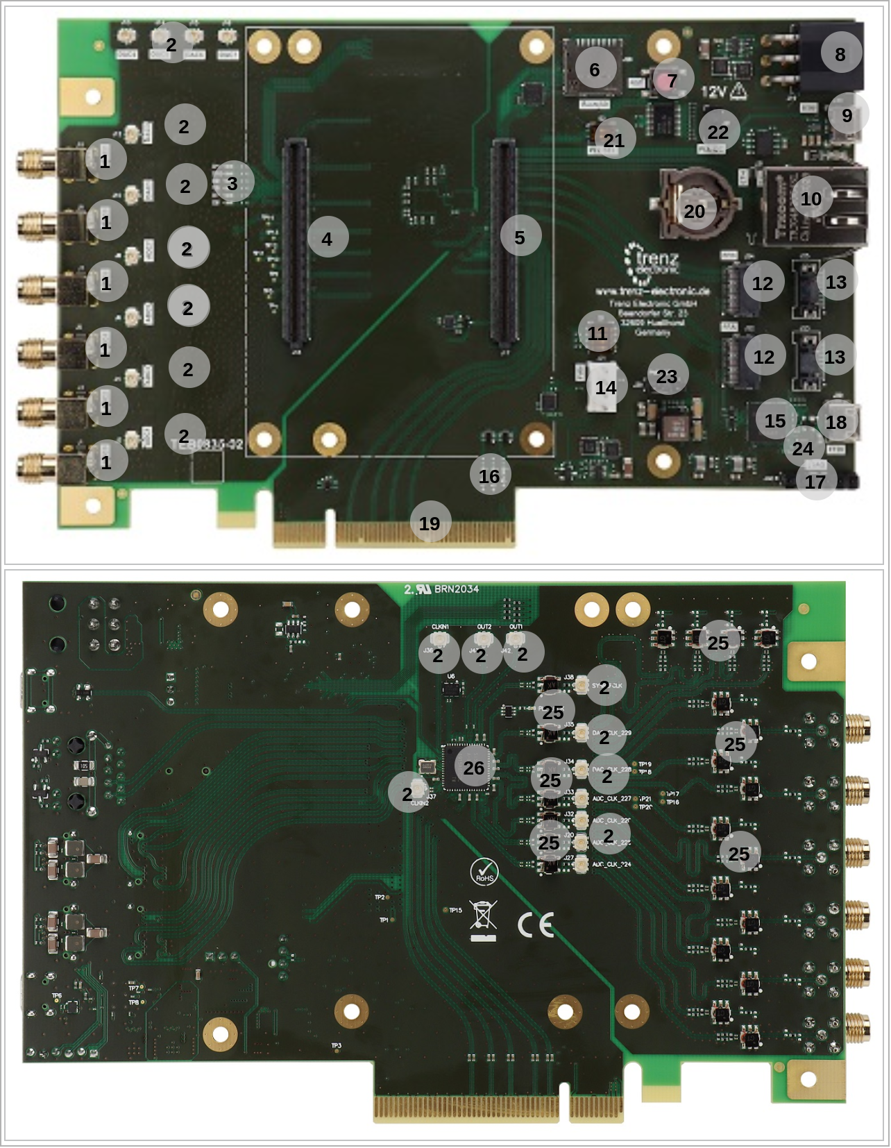
Notes : - Picture of the PCB (top and bottom side) with labels of important components
- Add List below
|
| Scroll Title |
|---|
| anchor | Figure_OV_MC |
|---|
| title | TEB0835 main components |
|---|
|
| Scroll Ignore |
|---|
| draw.io Diagram |
|---|
| border | false |
|---|
| viewerToolbar | true |
|---|
| |
|---|
| fitWindow | false |
|---|
| diagramDisplayName | |
|---|
| lbox | true |
|---|
| revision | 15 |
|---|
| diagramName | TEB0835_OV_MC |
|---|
| simpleViewer | false |
|---|
| width | 639 |
|---|
| links | auto |
|---|
| tbstyle | hidden |
|---|
| diagramWidth | 642 |
|---|
|
|
| Scroll Only |
|---|
|
|
- SMA Connectors, J1,J3,J5,J7,J9,J11
- UMCC Connectors, J2,J4,J6,J8, J10, J12...16, J20, J27, J32...J38, J42...43
- Green LEDs, D6...11
- B2B Connector, J18
- B2B Connector, J17
- Micro SD Card Connector, J28
- Reset Push Button, BTN1
- PCIe 6 Pin Connector, J19
- Micro USB2.0 Connectors, J30
- Gigabit RJ45 Connector, J31
- DIP Switch, S1
- UEC5 Connector, J22,J24
- UCC8 Connector, J23,J25
- 1x4 Pin Header, J21
- FTDI, U12
- Green LEDs, D1...3
- 1x6 Pin Header, J40
- Micro USB2.0 Connectors (FTDI), J29
- PCIe-8x-kurz Card, J26
- Battery Holder, B1
- DIP Switch (PLL SEL), S2
- Pin Header (PLL I2C), J41
- Jumper (PWR CFG), J39
- EEPROM, U15
- RF Transformer, T2...17, T26...32
- Programmable Clock Generator, U5
Initial Delivery State
| Page properties |
|---|
|
Notes : Only components like EEPROM, QSPI flash can be initialized by default at manufacture. If there is no components which might have initial data ( possible on carrier) you must keep the table empty |
| Scroll Title |
|---|
| anchor | Table_OV_IDS |
|---|
| title | Initial delivery state of programmable devices on the module |
|---|
|
| Scroll Table Layout |
|---|
| orientation | portrait |
|---|
| sortDirection | ASC |
|---|
| repeatTableHeaders | default |
|---|
| style | |
|---|
| widths | |
|---|
| sortByColumn | 1 |
|---|
| sortEnabled | false |
|---|
| cellHighlighting | true |
|---|
|
Storage device name | Content | Notes |
|---|
| EEPROM | Programmed | FTDI Configuration |
|
Configuration Signals
| Page properties |
|---|
|
- Overview of Boot Mode, Reset, Enables.
|
Push Button BTN1 is provided to switch OFF all power supplies on RFSoC board.
| Scroll Title |
|---|
| anchor | Table_OV_RST |
|---|
| title | Reset process. |
|---|
|
| Scroll Table Layout |
|---|
| orientation | portrait |
|---|
| sortDirection | ASC |
|---|
| repeatTableHeaders | default |
|---|
| style | |
|---|
| widths | |
|---|
| sortByColumn | 1 |
|---|
| sortEnabled | false |
|---|
| cellHighlighting | true |
|---|
|
Signal | B2B | I/O | Note |
|---|
RESETN | J17- 36 | Input | Connected to Push Button, BTN1 |
|
There is a DIP switch S1 provided for enabling CPLD and set the FPGA boot mode. The DIP Switch setting should be set like the following table.
| Scroll Title |
|---|
| anchor | Table_OV_DIP |
|---|
| title | CPLD Configuration |
|---|
|
| Scroll Table Layout |
|---|
| orientation | portrait |
|---|
| sortDirection | ASC |
|---|
| repeatTableHeaders | default |
|---|
| style | |
|---|
| widths | |
|---|
| sortByColumn | 1 |
|---|
| sortEnabled | false |
|---|
| cellHighlighting | true |
|---|
|
| DIP | Signal | Setting | Note |
|---|
| S1-A | CPLD_IO0 | FPGA boot config | Bit 0, CPLD Firmware dependent. | | S1-B | CPLD_IO1 | FPGA boot config | SDA pin | | S1-C | CPLD_IO2 | - | PROGRAMN pin | | S1-D | CPLD_JTAGEN | CPLD JTAG EN | JTAGENB |
|
Boot Mode must be set using DIP Switch S1 on CPLD provided on the module TE0835. Please note that the DIP Switch is active low.
| Scroll Title |
|---|
| anchor | Table_OV_BP |
|---|
| title | Boot process. |
|---|
|
| Scroll Table Layout |
|---|
| orientation | portrait |
|---|
| sortDirection | ASC |
|---|
| repeatTableHeaders | default |
|---|
| style | |
|---|
| widths | |
|---|
| sortByColumn | 1 |
|---|
| sortEnabled | false |
|---|
| cellHighlighting | true |
|---|
|
MODE Signal State | Boot Mode |
|---|
| S1-A | S1-B |
|---|
| JTAG | ON | ON | | QSPI Flash | ON | OFF | | SD Card | OFF | OFF |
|
Signals, Interfaces and Pins
| Page properties |
|---|
|
Notes : - For carrier or stand-alone boards use subsection for every connector type (add designator on description, not on the subsection title), for example:
- For modules which needs carrier use only classes and refer to B2B connector if more than one is used, for example
|
Board to Board (B2B) I/Os
Number of I/O signals and interfaces connected to the B2B connectors:
| Scroll Title |
|---|
| anchor | Table_SIP_B2B |
|---|
| title | B2B connections information |
|---|
|
| Scroll Table Layout |
|---|
| orientation | portrait |
|---|
| sortDirection | ASC |
|---|
| repeatTableHeaders | default |
|---|
| style | |
|---|
| widths | |
|---|
| sortByColumn | 1 |
|---|
| sortEnabled | false |
|---|
| cellHighlighting | true |
|---|
|
| B2B Connector | Interface | I/O Signal Count | Connected to | Notes |
|---|
J17
| I2C | 3x Single Ended | I2C Switch, U7 |
| PLL Intrupt PLL Clocks | 1x Single Ended 4x Single Ended, 2x Differential pairs | PLL Clock Generator, U5 |
| | JTAG | 4x Single Ended | FTDI, U12 |
| CPLD IO CPLD Enable | 3x Single Ended 1x Single Ended | DIP Switch, S1 |
| | PCIe Reset | 1x Single Ended | PCIe Card, J26 |
| | UART | 2x Single Ended | FTDI, U12 |
| Ethernet LED Ethernet MDI | 2x Single Ended 8x Single Ended | RJ45 Connector, J31 |
| | SD Card | 6x Single Ended | Micro SD Memory Connector, J28 IO Expander, U11 |
| | I/O | 16x Single Ended, 8x Differential pairs | PCIe Card, J26 | PCIe | | I/O | 16x Single Ended, 8x Differential pairs | UEC5 Connector, J22 | UEC5 | | I/O | 16x Single Ended, 8x Differential pairs | UEC5 Connector, J24 | UEC5 | | Micro USB2.0 | 2x Single Ended 1x Single Ended 2x Single Ended | Micro USB2.0 Connector, J30 Voltage Regulator, U17 Diode, D5 |
| | J18 | ADC | 16x Single Ended, 8x Differential pairs | SMA, J1, J3, J5, J7 UMCC, J2, J4, J6, J8 |
| | ADC Clock | 4x Single Ended, 2x Differential pairs | UMCC, J27, J32 |
| | DAC | 16x Single Ended, 8x Differential pairs
| SMA, J9, J11 UMCC, J10, J12, J13...16 |
| | DAC Clock | 4x Single Ended, 2x Differential pairs | UMCC, J33, J34 |
| | Green LEDs | 6x Single Ended, 3x Differential pairs | Green LEDs, D6...11 |
| | I/O | 10x Single Ended | UCC8 Connector, J23, J25 | UCC8 |
|
Gigabit Ethernet
| Scroll Title |
|---|
| anchor | Table_SIP_ETH |
|---|
| title | Gigabit Ethernet information |
|---|
|
| Scroll Table Layout |
|---|
| orientation | portrait |
|---|
| sortDirection | ASC |
|---|
| repeatTableHeaders | default |
|---|
| style | |
|---|
| widths | |
|---|
| sortByColumn | 1 |
|---|
| sortEnabled | false |
|---|
| cellHighlighting | true |
|---|
|
| Signal Name | Connected to | Signal Description | Note |
|---|
| PHY_MDI0...3 | B2B, J17 | Media Data |
| | PHY_LED0...1 | B2B, J17 | Speed/Link Indicators LED | Yellow/Green |
|
Micro USB for JTAG/UART
The TEB0835 is equipped with two Micro USB2.0 Connectors J29, J30. The Micro USB2.0 port, J29 is provided for JTAG/UART and it is connected to FTDI, U12.
| Scroll Title |
|---|
| anchor | Table_SIP_MUSB2 |
|---|
| title | Micro USB2 to JTAG/UART connections |
|---|
|
| Scroll Table Layout |
|---|
| orientation | portrait |
|---|
| sortDirection | ASC |
|---|
| repeatTableHeaders | default |
|---|
| style | |
|---|
| widths | |
|---|
| sortByColumn | 1 |
|---|
| sortEnabled | false |
|---|
| cellHighlighting | true |
|---|
|
| Designator | Signal Name | Connected to | Note |
|---|
| J29 | D_N/D_P | FTDI,U12 | Data | | USB_VBUS | Diode, D4 | VBUS |
|
Micro USB2.0
There is a Micro USB2.0 J30, provided for user.
| Scroll Title |
|---|
| anchor | Table_SIP_MicroUSB2 |
|---|
| title | Micro USB2.0 Socket connections |
|---|
|
| Scroll Table Layout |
|---|
| orientation | portrait |
|---|
| sortDirection | ASC |
|---|
| repeatTableHeaders | default |
|---|
| style | |
|---|
| widths | |
|---|
| sortByColumn | 1 |
|---|
| sortEnabled | false |
|---|
| cellHighlighting | true |
|---|
|
| Designator | Signal Name | Connected to | Note |
|---|
J30
| USB_N/USB_P | B2B, J17 | Data | | USB0_VBUS | B2B, J17 | VBUS | | USB0_ID | B2B, J17 | ID |
|
Micro SD Card Reader
There is a Micro SD Card socket J28 connected to B2B J17 through an I/O expander U11.
| Scroll Title |
|---|
| anchor | Table_SIP_MicroSD |
|---|
| title | Micro SD Card Socket connections |
|---|
|
| Scroll Table Layout |
|---|
| orientation | portrait |
|---|
| sortDirection | ASC |
|---|
| repeatTableHeaders | default |
|---|
| style | |
|---|
| widths | |
|---|
| sortByColumn | 1 |
|---|
| sortEnabled | false |
|---|
| cellHighlighting | true |
|---|
|
| Pin | Signal Name | Connected to | Note |
|---|
| VDD | 3.3V_SD | B2B, J17 | connected to IO expander | | CMD | SD_CMD | B2B, J17 | connected to IO expander | | CLK | SD_CLK | B2B, J17 | connected to IO expander | | DATA0...3 | SD_DATA0...3 | B2B, J17 | connected to IO expander | | CD | SD_CD | B2B, J17 |
|
|
SMA Connectors
There are 6 SMA Connectors provided for Analog and Digital signals.
| Scroll Title |
|---|
| anchor | Table_SIP_SMA |
|---|
| title | SMA Connectors information |
|---|
|
| Scroll Table Layout |
|---|
| orientation | portrait |
|---|
| sortDirection | ASC |
|---|
| repeatTableHeaders | default |
|---|
| style | |
|---|
| widths | |
|---|
| sortByColumn | 1 |
|---|
| sortEnabled | false |
|---|
| cellHighlighting | true |
|---|
|
| Designator | Signal Name | Connected to | Note |
|---|
| J1 | ADC0_IN | B2B, J18 | Via RF Transformer T2 | | J3 | ADC2_IN | B2B, J18 | Via RF Transformer T6 | | J5 | ADC4_IN | B2B, J18 | Via RF Transformer T4 | | J7 | ADC6_IN | B2B, J18 | Via RF Transformer T8 | | J9 | DAC0_OUT | B2B, J18 | Via RF Transformer T10 | | J11 | DAC2_OUT | B2B, J18 | Via RF Transformer T12 |
|
UMCC Connectors
There are 21x UMCC Connectors provided for Analog /Digital signals and Clocks input and output.
| Scroll Title |
|---|
| anchor | Table_SIP_UMCC |
|---|
| title | UMCC Connectors |
|---|
|
| Scroll Table Layout |
|---|
| orientation | portrait |
|---|
| sortDirection | ASC |
|---|
| repeatTableHeaders | default |
|---|
| style | |
|---|
| widths | |
|---|
| sortByColumn | 1 |
|---|
| sortEnabled | false |
|---|
| cellHighlighting | true |
|---|
|
| Designator | Signal Name | Connected to | Note |
|---|
| J2 | ADC1_IN | B2B, J18 | Via RF Transformer T3 | | J4 | ADC3_IN | B2B, J18 | Via RF Transformer T5 | | J6 | ADC5_IN | B2B, J18 | Via RF Transformer T7 | | J8 | ADC7_IN | B2B, J18 | Via RF Transformer T9 | | J10 | DAC1_OUT | B2B, J18 | Via RF Transformer T11 | | J12 | DAC3_OUT | B2B, J18 | Via RF Transformer T13 | | J13 | DAC4_OUT | B2B, J18 | Via RF Transformer T14 | | J14 | DAC5_OUT | B2B, J18 | Via RF Transformer T15 | | J15 | DAC6_OUT | B2B, J18 | Via RF Transformer T16 | | J16 | DAC7_OUT | B2B, J18 | Via RF Transformer T17 | | J27 | ADC_CLK_224 | B2B, J18 | Via RF Transformer T26 | | J20 | ADC_CLK_225 | B2B, J18 | Via RF Transformer T27 | | J32 | ADC_CLK_226 | B2B, J18 | Via RF Transformer T28 | | J33 | ADC_CLK_227 | B2B, J18 | Via RF Transformer T29 | | J34 | DAC_CLK_228 | B2B, J18 | Via RF Transformer T30 | | J35 | DAC_CLK_229 | B2B, J18 | Via RF Transformer T31 | | J36 | CLKIN1 | Programmable Clock Generator, U5 |
| | J37 | CLKIN2 | Programmable Clock Generator, U5 |
| | J38 | CLKOUT7 | Programmable Clock Generator, U5 | Via RF Transformer T32 | | J42 | CLKOUT8 | Programmable Clock Generator, U5 |
| | J43 | CLKOUT9 | Programmable Clock Generator, U5 |
|
|
UCE5 Connectors
The TEB0835 is equipped with two UCE5 Connectors.
| Scroll Title |
|---|
| anchor | Table_SIP_UEC5 |
|---|
| title | UEC5 Connectors |
|---|
|
| Scroll Table Layout |
|---|
| orientation | portrait |
|---|
| sortDirection | ASC |
|---|
| repeatTableHeaders | default |
|---|
| style | |
|---|
| widths | |
|---|
| sortByColumn | 1 |
|---|
| sortEnabled | false |
|---|
| cellHighlighting | true |
|---|
|
| Designator | Signal Name | Connected to | Note |
|---|
| J22 | B128_TX0...3 | B2B, J17 | 8x Single Ended/ 4x LVDS Pairs | | B128_RX0...3 | B2B, J17 | 8x Single Ended/ 4x LVDS Pairs | | J24 | B129_TX0...3 | B2B, J17 | 8x Single Ended/ 4x LVDS Pairs | | B129_RX0...3 | B2B, J17 | 8x Single Ended/ 4x LVDS Pairs |
|
UCC8 Connectors
The TEB0835 is equipped with two UCC8 Connectors.
| Scroll Title |
|---|
| anchor | Table_SIP_UCC8 |
|---|
| title | UCC8 Connectors |
|---|
|
| Scroll Table Layout |
|---|
| orientation | portrait |
|---|
| sortDirection | ASC |
|---|
| repeatTableHeaders | default |
|---|
| style | |
|---|
| widths | |
|---|
| sortByColumn | 1 |
|---|
| sortEnabled | false |
|---|
| cellHighlighting | true |
|---|
|
| Designator | Signal Name | Connected to | Note |
|---|
| J23 | FFA_MPRS | B2B, J17 |
| | FFA_MSEL | B2B, J17 |
| | FFA_INTL | B2B, J17 |
| | FFA_RSTL | B2B, J17 |
| | FFA_SCL/FFA_SDA | I2C Switch, U7 |
| | J25 | FFB_MPRS | B2B, J17 |
| | FFB_MSEL | B2B, J17 |
| | FFB_INTL | B2B, J17 |
| | FFB_RSTL | B2B, J17 |
| | FFB_SCL/FFB_SDA | I2C Switch, U7 |
|
|
PCIe 8x Short
There is a PICe-8x-Short card provided on the TEB0835 board.
| Scroll Title |
|---|
| anchor | Table_SIP_PCIe |
|---|
| title | PCIe x8 Kurz Connections |
|---|
|
| Scroll Table Layout |
|---|
| orientation | portrait |
|---|
| sortDirection | ASC |
|---|
| repeatTableHeaders | default |
|---|
| style | |
|---|
| widths | |
|---|
| sortByColumn | 1 |
|---|
| sortEnabled | false |
|---|
| cellHighlighting | true |
|---|
|
| Signal Name | Connected to | Note |
|---|
| B505_RX0...3 | B2B, J17 | 8x Single Ended/ 4x LVDS Pairs | | B505_TX0...3 | B2B, J17 | 8x Single Ended/ 4x LVDS Pairs | | EXT_CLKIN_PSMGT | B2B, J17 |
| | PCIE_RSTB_R | B2B, J17 | Pulled up to 1.8V |
|
PCIe 6 Pins
| Scroll Title |
|---|
| anchor | Table_SIP_PCIe1x6 |
|---|
| title | PCIe 1x6 Connection |
|---|
|
| Scroll Table Layout |
|---|
| orientation | portrait |
|---|
| sortDirection | ASC |
|---|
| repeatTableHeaders | default |
|---|
| style | |
|---|
| widths | |
|---|
| sortByColumn | 1 |
|---|
| sortEnabled | false |
|---|
| cellHighlighting | true |
|---|
|
| Pin | Signal Name | Connected to | Note |
|---|
| 1 | 12V_input_A | Regulator, U2
|
| | 2 | | 3 | | 4 | GND | N.C |
| | 5 | | 6 |
|
| Scroll Title |
|---|
| anchor | Table_SIP_PinHeader1x4 |
|---|
| title | Pin Header1x4 Connections |
|---|
|
| Scroll Table Layout |
|---|
| orientation | portrait |
|---|
| sortDirection | ASC |
|---|
| repeatTableHeaders | default |
|---|
| style | |
|---|
| widths | |
|---|
| sortByColumn | 1 |
|---|
| sortEnabled | false |
|---|
| cellHighlighting | true |
|---|
|
| Pin | Signal Name | Connected to | Note |
|---|
| 1 | GND | GND |
| | 2 | FAN_PWR | 12V |
| | 3 | FAN_TACH | Tepmerature Sensor, U9 |
| | 4 | FAN_PWM | Tepmerature Sensor, U9 |
|
|
There is a 1x6 Pin Header J40, connected to JTAG signals as the following.
| Scroll Title |
|---|
| anchor | Table_SIP_PinHeader1x6 |
|---|
| title | Pin Header1x6 Connections |
|---|
|
| Scroll Table Layout |
|---|
| orientation | portrait |
|---|
| sortDirection | ASC |
|---|
| repeatTableHeaders | default |
|---|
| style | |
|---|
| widths | |
|---|
| sortByColumn | 1 |
|---|
| sortEnabled | false |
|---|
| cellHighlighting | true |
|---|
|
| Pin | Signal Name | Connected to | Note |
|---|
| 1 | JTAG_TMS | B2B, J17 FTDI, U12 |
| | 2 | JTAG_TDI | B2B, J17 FTDI, U12 |
| | 3 | JTAG_TDO | B2B, J17 FTDI, U12 |
| | 4 | JTAG_TCK | B2B, J17 FTDI, U12 |
| | 5 | GND | - |
| | 6 | 3.3V_MODULE | B2B, J17 |
|
|
There is a 1x3 Pin Header J41, it provides access to I2C signals which are connected to I2C Switch, U7.
| Scroll Title |
|---|
| anchor | Table_SIP_PinHeder1x3 |
|---|
| title | Pin Header 1x3 Connectors |
|---|
|
| Scroll Table Layout |
|---|
| orientation | portrait |
|---|
| sortDirection | ASC |
|---|
| repeatTableHeaders | default |
|---|
| style | |
|---|
| widths | |
|---|
| sortByColumn | 1 |
|---|
| sortEnabled | false |
|---|
| cellHighlighting | true |
|---|
|
| Pin | Signal Name | Connected to | Note |
|---|
| 1 | DSPLL0_SCL | I2C Switch, U7 |
| | 2 | GND | I2C Switch, U7 |
| | 3 | DSPLL0_SCL | I2C Switch, U7 |
|
|
Jumper
There is a Jumper J39 provided for setting the DCDC_EN between two signal level as the following.
| Scroll Title |
|---|
| anchor | Table_SIP_Jumper |
|---|
| title | Jumper Connections |
|---|
|
| Scroll Table Layout |
|---|
| orientation | portrait |
|---|
| sortDirection | ASC |
|---|
| repeatTableHeaders | default |
|---|
| style | |
|---|
| widths | |
|---|
| sortByColumn | 1 |
|---|
| sortEnabled | false |
|---|
| cellHighlighting | true |
|---|
|
| Pin | Signal Name | Connected to | Note |
|---|
| 1 | PG_5V | Regulator, U8 |
| | 2 | DCDC_EN | Regulator, U1, U4 |
| | 3 | MODULE_PG | B2B, J17 |
|
|
I2C Addresses
| Scroll Title |
|---|
| anchor | Table_OBP_I2C_ADD |
|---|
| title | I2C addresses table |
|---|
|
| Scroll Table Layout |
|---|
| orientation | portrait |
|---|
| sortDirection | ASC |
|---|
| repeatTableHeaders | default |
|---|
| style | |
|---|
| widths | |
|---|
| sortByColumn | 1 |
|---|
| sortEnabled | false |
|---|
| cellHighlighting | true |
|---|
|
| Designator | I2C Address | Notes |
|---|
| U9 | 0x4C | Temperature Sensor IC | | U7 | 0x70 | I2C Switch | | U5 | 0x68 | Programmable Clock Generator |
|
Test Points
| Page properties |
|---|
|
you must fill the table below with group of Test Point which are indicated as TP in a schematic. If there is no Test Point remarked in the schematic, delet the Test Point section. Example: | Test Point | Signal | B2B | Notes |
|---|
| 10 | PWR_PL_OK | J2-120 |
|
|
| Scroll Title |
|---|
| anchor | Table_SIP_TPs |
|---|
| title | Test Points Information |
|---|
|
| Scroll Table Layout |
|---|
| orientation | portrait |
|---|
| sortDirection | ASC |
|---|
| repeatTableHeaders | default |
|---|
| style | |
|---|
| widths | |
|---|
| sortByColumn | 1 |
|---|
| sortEnabled | false |
|---|
| cellHighlighting | true |
|---|
|
| Test Point | Signal | Connected to | Notes |
|---|
| TP1 | 5V | B2B, J17 |
| | TP2...3 | GND | GND |
| | TP4 | ADC0_VCM | B2B, J18 |
| | TP5 | ADC1_VCM | B2B, J18 |
| | TP6 | USB_VBUS | Micro USB2.0, J29 |
| | TP7 | UART0_RX | B2B, J17 |
| | TP8 | UART0_TX | B2B, J17 |
| | TP9 | ADC2_VCM | B2B, J18 |
| | TP10 | ADC3_VCM | B2B, J18 |
| | TP11 | ADC4_VCM | B2B, J18 |
| | TP12 | ADC5_VCM | B2B, J18 |
| | TP13 | ADC6_VCM | B2B, J18 |
| | TP14 | ADC7_VCM | B2B, J18 |
| | TP15 | PSBATT | Diode, D13 |
| | TP16 | CLKE_P | - |
| | TP17 | CLKE_N | - |
| | TP18 | CLKF_P | - |
| | TP19 | CLKF_N | - |
| | TP20 | CLKD_P | - |
| | TP21 | CLKD_N | - |
|
|
On-board Peripherals
| Page properties |
|---|
|
Notes : - add subsection for every component which is important for design, for example:
- Two 100 Mbit Ethernet Transciever PHY
- USB PHY
- Programmable Clock Generator
- Oscillators
- eMMCs
- RTC
- FTDI
- ...
- DIP-Switches
- Buttons
- LEDs
|
| Page properties |
|---|
|
Notes : In the on-board peripheral table "chip/Interface" must be linked to the corresponding chapter or subsection |
| Scroll Title |
|---|
| anchor | Table_OBP |
|---|
| title | On board peripherals |
|---|
|
| Scroll Table Layout |
|---|
| orientation | portrait |
|---|
| sortDirection | ASC |
|---|
| repeatTableHeaders | default |
|---|
| style | |
|---|
| widths | |
|---|
| sortByColumn | 1 |
|---|
| sortEnabled | false |
|---|
| cellHighlighting | true |
|---|
|
|
EEPROM
There is an EEPROM U15 provided in order to store the FTDI configuration.
| Scroll Title |
|---|
| anchor | Table_OBP_EEP |
|---|
| title | EEPROM information |
|---|
|
| Scroll Table Layout |
|---|
| orientation | portrait |
|---|
| sortDirection | ASC |
|---|
| repeatTableHeaders | default |
|---|
| style | |
|---|
| widths | |
|---|
| sortByColumn | 1 |
|---|
| sortEnabled | false |
|---|
| cellHighlighting | true |
|---|
|
| Pin | Schematic | Connected to | Notes |
|---|
| CS | EECS | FTDI, U12 |
| | CLK | EECLK | FTDI, U12 |
| | DIN | EEDATA | FTDI, U12 |
|
|
DIP Switch
There are two DIP Switches S1, S2 provided for boot mode and manual input select of programmable clock generator. For more information please refer to Configuration Signal Section
| Scroll Title |
|---|
| anchor | Table_OBP_DIP |
|---|
| title | DIP Switches information |
|---|
|
| Scroll Table Layout |
|---|
| orientation | portrait |
|---|
| sortDirection | ASC |
|---|
| repeatTableHeaders | default |
|---|
| style | |
|---|
| widths | |
|---|
| sortByColumn | 1 |
|---|
| sortEnabled | false |
|---|
| cellHighlighting | true |
|---|
|
| Designator | Pin | Schematic | Connected to | Notes |
|---|
| S1 | S1A | CPLD_IO0 | B2B, J17 |
| | S1B | CPLD_IO1 | B2B, J17 |
| | S1C | CPLD_IO2 | B2B, J17 |
| | S1D | CPLD_JTAGEN | B2B, J17 |
| | S2 | S2A | DSPLL0_SEL0 | Programmable clock Generator, U5 |
| | S2B | DSPLL0_SEL0 | Programmable clock Generator, U5 |
|
|
Temperature Sensor
There is a temperature sensor IC U9 provided to capture the temperature and provides an alert when cooling is needed. the temperature IC is connected to I2C bus at address 0x4C.
| Scroll Title |
|---|
| anchor | Table_OBP_Temp |
|---|
| title | Temperature sensor information |
|---|
|
| Scroll Table Layout |
|---|
| orientation | portrait |
|---|
| sortDirection | ASC |
|---|
| repeatTableHeaders | default |
|---|
| style | |
|---|
| widths | |
|---|
| sortByColumn | 1 |
|---|
| sortEnabled | false |
|---|
| cellHighlighting | true |
|---|
|
| Pin | Schematic | Connected to | Notes |
|---|
| TACH | FAN_TACH | Pin Header, J21 |
| | PWM | FAN_PWM | Pin Header, J21 |
| | D+ | DX_P | Regulator, U8 |
| | D- | DX_N | Regulator, U8 |
| | nALERT | ALERT_N | I2C Switch, U7 |
| | nTCRIT | THERM_N | pulled up to 3.3V |
| | SMBCLK | I2C_SCL_SNS | I2C Switch, U7 |
| | SMBDAT | I2C_SDA_SNS | I2C Switch, U7 |
|
|
FTDI
The FTDI chip U12 converts signals from USB2 to a variety of standard serial and parallel interfaces. Refer to the FTDI data sheet to get information about the capacity of the FT2232H chip. FTDI FT2232H chip is used in MPPSE mode for JTAG, 2 I/O's of Channel B are routed to B2B J17 and must be used as UART.
The configuration of FTDI FT2232H chip is pre-programmed on the EEPROM U15.
| Scroll Title |
|---|
| anchor | Table_OBP_FTDI |
|---|
| title | FTDI chip interfaces and pins |
|---|
|
| Scroll Table Layout |
|---|
| orientation | portrait |
|---|
| sortDirection | ASC |
|---|
| repeatTableHeaders | default |
|---|
| sortByColumn | 1 |
|---|
| sortEnabled | false |
|---|
| cellHighlighting | true |
|---|
|
| FTDI Pin | Signal Schematic Name | Connected to | Notes |
|---|
| ADBUS0 | JTAG_TCK | B2B, J17 Pin Header, J40 | JTAG interface | | ADBUS1 | JTAG_TDI | B2B, J17 Pin Header, J40 | | ADBUS2 | JTAG_TDO | B2B, J17 Pin Header, J40 | | ADBUS3 | JTAG_TMS | B2B, J17 Pin Header, J40 | | BDBUS0 | UART0_RX | B2B, J17 | UART | | BDBUS1 | UART0_TX | B2B, J17 | UART | | EECS/EECLK/EEDATA | BDBUS2 | EEPROM, U15 | FTDI configuration | | DM/DP | D_N/D_P | Micro USB2.0, J29 | FTDI Input |
|
| Scroll Title |
|---|
| anchor | Table_OBP_BTN |
|---|
| title | Push Button information |
|---|
|
| Scroll Table Layout |
|---|
| orientation | portrait |
|---|
| sortDirection | ASC |
|---|
| repeatTableHeaders | default |
|---|
| style | |
|---|
| widths | |
|---|
| sortByColumn | 1 |
|---|
| sortEnabled | false |
|---|
| cellHighlighting | true |
|---|
|
| Designator | Connected to | Functionality | Note |
|---|
| BTN1 | RESETN | General Reset |
|
|
LEDs
| Scroll Title |
|---|
| anchor | Table_OBP_LED |
|---|
| title | On-board LEDs |
|---|
|
| Scroll Table Layout |
|---|
| orientation | portrait |
|---|
| sortDirection | ASC |
|---|
| repeatTableHeaders | default |
|---|
| style | |
|---|
| widths | |
|---|
| sortByColumn | 1 |
|---|
| sortEnabled | false |
|---|
| cellHighlighting | true |
|---|
|
| Designator | Color | Connected to | Active Level | Note |
|---|
| D1 | Green | PG_1.8V | High |
| | D2 | Green | PG_3.3V | High |
| | D3 | Green | PG_5V | High |
| | D6...11 | Green | B2B, J18 | High | User LED | | D12 | Green | Clock Generator, U5 | High |
|
|
Clock Sources
| Scroll Title |
|---|
| anchor | Table_OBP_CLK |
|---|
| title | Osillators |
|---|
|
| Scroll Table Layout |
|---|
| orientation | portrait |
|---|
| sortDirection | ASC |
|---|
| repeatTableHeaders | default |
|---|
| style | |
|---|
| widths | |
|---|
| sortByColumn | 1 |
|---|
| sortEnabled | false |
|---|
| cellHighlighting | true |
|---|
|
| Designator | Description | Frequency | Note |
|---|
| U6 | MEMS Oscillator | 100 MHz |
| | U16 | MEMS Oscillator | 12 MHz |
| | Y1 | Crystal Oscillator | 54 MHz |
| | U5 | Programmable Clock Generator | Variable |
|
|
Programmable Clock Generator
There is a programmable clock generator on-board (U5) provided in order to generate variable clocks for the module. The I2C Address is 0x68.
| Scroll Title |
|---|
| anchor | Table_OBP_PCLK |
|---|
| title | Programmable Clock Generator Inputs and Outputs |
|---|
|
| Scroll Table Layout |
|---|
| orientation | portrait |
|---|
| sortDirection | ASC |
|---|
| repeatTableHeaders | default |
|---|
| sortByColumn | 1 |
|---|
| sortEnabled | false |
|---|
| cellHighlighting | true |
|---|
|
U5 Pin
| Signal | Connected to | Direction | Note |
|---|
| IN0 | CLKIN0 | Oscillator, U6 | Input |
| | IN1 | CLKIN1 | UMCC Connector, J36 | Input |
| | IN2 | CLKIN2 | UMCC Connector, J37 | Input |
| | IN3 | FB | Programmable Clock Generator, U5 | Input/Output |
| | XA/XB | CLK0_XA/XB | Oscillator, Y1 | Input |
| | IN_SEL0...1 | DSPLL0_SEL0...1 | I2C Switch, U7 DIP Switch, S2 | Input |
| | nINTR | DSPLL0_INTR_N | I2C Switch, U7 | Input |
| | nLOL | DSPLL0_LOL_N | Green LED, D12 | Input |
| | nRST | DSPLL0_RST_N | 1.8 V | Input |
| | SCLK | DSPLL0_SCL | I2C Switch, U7 | Input |
| | SDA/SDIO | DSPLL0_SDA | I2C Switch, U7 Pin Header, J41 | In/Out |
| | INTR | PLL_INTR_N | B2B, J17 | Output |
| | OUT0A | CLKOUT0A | B2B, J17 | Output |
| | OUT0 | CLKOUT0_P | B2B, J17 | Output |
| | OUT1 | PLLCLK1 | UMMC, J27 | Output |
| | OUT2 | PLLCLK2 | UMMC, J20 | Output |
| | OUT3 | PLLCLK3 | UMMC, J32 | Output |
| | OUT4 | PLLCLK4 | UMMC, J33 | Output |
| | OUT5 | PLLCLK5 | UMMC, J34 | Output |
| | OUT6 | PLLCLK6 | UMMC, J35 | Output |
| | OUT7 | CLKOUT7 | UMMC, J38 | Output |
| | OUT8 | CLKOUT8 | UMMC, J42 | Output |
| | OUT9 | CLKOUT9 | UMMC, J43 | Output |
| | OUT9A | CLKOUT9A | Programmable Clock Generator, U5 | Output |
|
|
Power and Power-On Sequence
| Page properties |
|---|
|
In 'Power and Power-on Sequence' section there are three important digrams which must be drawn: - Power on-sequence
- Power distribution
- Voltage monitoring circuit
|
Power Supply
Power supply with minimum current capability of 3 A for system startup is recommended.
Power Consumption
| Scroll Title |
|---|
| anchor | Table_PWR_PC |
|---|
| title | Power Consumption |
|---|
|
| Scroll Table Layout |
|---|
| orientation | portrait |
|---|
| sortDirection | ASC |
|---|
| repeatTableHeaders | default |
|---|
| style | |
|---|
| widths | |
|---|
| sortByColumn | 1 |
|---|
| sortEnabled | false |
|---|
| cellHighlighting | true |
|---|
|
| Power Input Pin | Typical Current |
|---|
| VIN | TBD* |
|
* TBD - To Be Determined
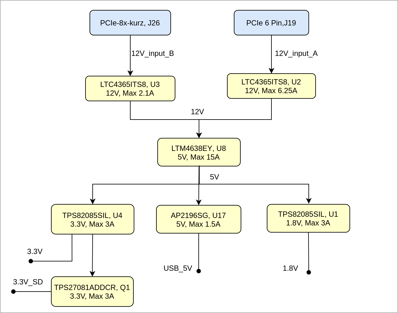
Power Distribution Dependencies
| Scroll Title |
|---|
| anchor | Figure_PWR_PD |
|---|
| title | Power Distribution |
|---|
|
| Scroll Ignore |
|---|
| draw.io Diagram |
|---|
| border | false |
|---|
| viewerToolbar | true |
|---|
| |
|---|
| fitWindow | false |
|---|
| diagramDisplayName | |
|---|
| lbox | true |
|---|
| revision | 13 |
|---|
| diagramName | TEB0835_PWR_PD |
|---|
| simpleViewer | false |
|---|
| width | 639 |
|---|
| links | auto |
|---|
| tbstyle | hidden |
|---|
| diagramWidth | 640 |
|---|
|
|
| Scroll Only |
|---|
|
|
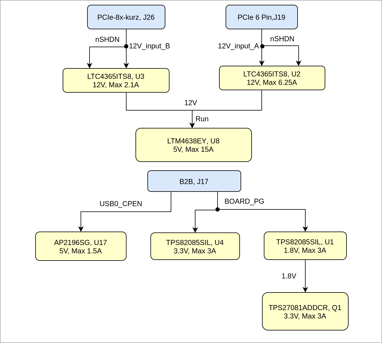
Power-On Sequence
| Scroll Title |
|---|
| anchor | Figure_PWR_PS |
|---|
| title | Power Sequency |
|---|
|
| Scroll Ignore |
|---|
| draw.io Diagram |
|---|
| border | false |
|---|
| |
|---|
| diagramName | TEB0835_PWR_PS |
|---|
| simpleViewer | false |
|---|
| width | 639 |
|---|
| links | auto |
|---|
| tbstyle | hidden |
|---|
| diagramDisplayName | |
|---|
| lbox | true |
|---|
| diagramWidth | 640 |
|---|
| revision | 2 |
|---|
|
|
| Scroll Only |
|---|
|
|
Power Rails
| Scroll Title |
|---|
| anchor | Table_PWR_PR |
|---|
| title | Module power rails. |
|---|
|
| Scroll Table Layout |
|---|
| orientation | portrait |
|---|
| sortDirection | ASC |
|---|
| repeatTableHeaders | default |
|---|
| style | |
|---|
| widths | |
|---|
| sortByColumn | 1 |
|---|
| sortEnabled | false |
|---|
| cellHighlighting | true |
|---|
|
| Power Rail Name | B2B JM17 | B2B JM2 | Direction | Notes |
|---|
| 5V | 1,2,3,4,5,6,8 | - | Ouput |
| | PSBATT | 14 | - | Output |
| | 3.3V_MODULE | 16 | - | Input |
|
|
Board to Board Connectors
| Page properties |
|---|
|
- This section is optional and only for modules.
use "include page" macro and link to the general B2B connector page of the module series, For example: 6 x 6 SoM LSHM B2B Connectors
| Include Page |
|---|
| 6 x 6 SoM LSHM B2B Connectors |
|---|
| 6 x 6 SoM LSHM B2B Connectors |
|---|
|
|
| Include Page |
|---|
| DRAFT:6.5 x 9 SoM SS5/ST5 B2B Connectors |
|---|
| DRAFT:6.5 x 9 SoM SS5/ST5 B2B Connectors |
|---|
|
Technical Specifications
Absolute Maximum Ratings
| Scroll Title |
|---|
| anchor | Table_TS_AMR |
|---|
| title | PS absolute maximum ratings |
|---|
|
| Scroll Table Layout |
|---|
| orientation | portrait |
|---|
| sortDirection | ASC |
|---|
| repeatTableHeaders | default |
|---|
| style | |
|---|
| widths | |
|---|
| sortByColumn | 1 |
|---|
| sortEnabled | false |
|---|
| cellHighlighting | true |
|---|
|
| Symbols | Description | Min | Max | Unit |
|---|
| VIN | Input Supply Voltage | 2.5 | 34 | V | | ADC_V | Analog input voltage | -5.0 | 5.0 | V | | DAC_V | Digital input voltage | -5.0 | 5.0 | °C | | T_STG | Storage Temperature | -55 | 125 | °C |
|
Recommended Operating Conditions
Operating temperature range depends also on customer design and cooling solution. Please contact us for options.
| Scroll Title |
|---|
| anchor | Table_TS_ROC |
|---|
| title | Recommended operating conditions. |
|---|
|
| Scroll Table Layout |
|---|
| orientation | portrait |
|---|
| sortDirection | ASC |
|---|
| repeatTableHeaders | default |
|---|
| style | |
|---|
| widths | |
|---|
| sortByColumn | 1 |
|---|
| sortEnabled | false |
|---|
| cellHighlighting | true |
|---|
|
| Parameter | Min | Max | Units | Reference Document |
|---|
| VIN | 11 | 13 | V | See the datasheet. | | ADC_V | 0 | 5 | V | See the SMA datasheet | | DAC_V | 0 | 5 | V | See the UMCC datasheet | | T_OPT | -40 | +85 | °C | See RF Transformer datasheet. |
|
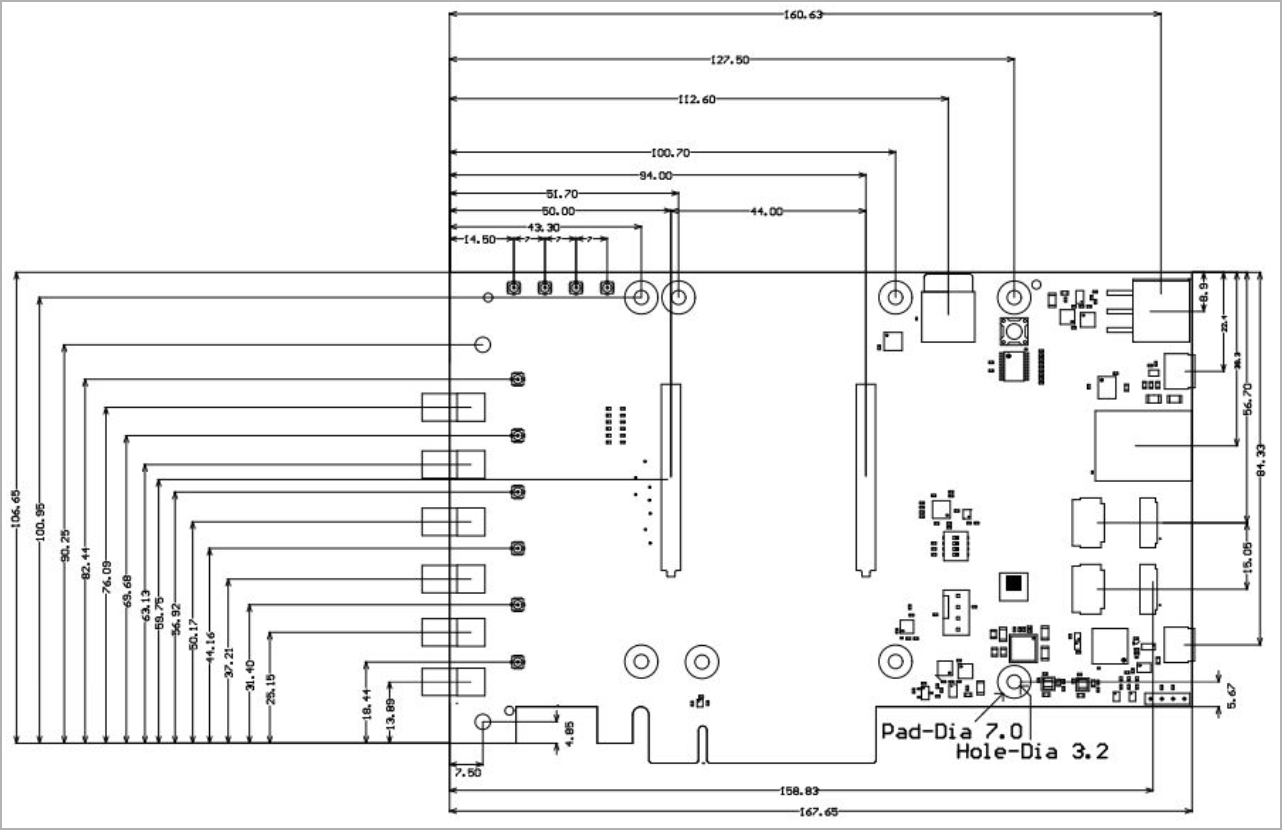
Physical Dimensions
PCB thickness: 1.5 mm.
| Scroll Title |
|---|
| anchor | Figure_TS_PD |
|---|
| title | Physical Dimension |
|---|
|
| Scroll Ignore |
|---|
| draw.io Diagram |
|---|
| border | false |
|---|
| viewerToolbar | true |
|---|
| |
|---|
| fitWindow | false |
|---|
| diagramDisplayName | |
|---|
| lbox | true |
|---|
| revision | 2 |
|---|
| diagramName | TEB0835_TS_PD |
|---|
| simpleViewer | false |
|---|
| width | 639 |
|---|
| links | auto |
|---|
| tbstyle | hidden |
|---|
| diagramWidth | 641 |
|---|
|
|
| Scroll Only |
|---|
| scroll-pdf | true |
|---|
| scroll-office | true |
|---|
| scroll-chm | true |
|---|
| scroll-docbook | true |
|---|
| scroll-eclipsehelp | true |
|---|
| scroll-epub | true |
|---|
| scroll-html | true |
|---|
| 
|
|
Currently Offered Variants
| Scroll Title |
|---|
| anchor | Table_VCP_SO |
|---|
| title | Trenz Electronic Shop Overview |
|---|
|
| Scroll Table Layout |
|---|
| orientation | portrait |
|---|
| sortDirection | ASC |
|---|
| repeatTableHeaders | default |
|---|
| style | |
|---|
| widths | |
|---|
| sortByColumn | 1 |
|---|
| sortEnabled | false |
|---|
| cellHighlighting | true |
|---|
|
|
Revision History
Hardware Revision History
| Scroll Title |
|---|
| anchor | Table_RH_HRH |
|---|
| title | Hardware Revision History |
|---|
|
| Scroll Table Layout |
|---|
| orientation | portrait |
|---|
| sortDirection | ASC |
|---|
| repeatTableHeaders | default |
|---|
| style | |
|---|
| widths | |
|---|
| sortByColumn | 1 |
|---|
| sortEnabled | false |
|---|
| cellHighlighting | true |
|---|
|
| Date | Revision | Changes | Documentation Link |
|---|
| 2019-11-29 | REV01 | Initial Release | REV01 | | 2020-08-13 | REV02 | - All module's mount holes are connected to GND;
- CLK_Connectors. Added baluns for each clock inputs;
- Internal DSPLL is changed on SI5395A-A-GM;
- Added ability to use internal DSPLL as a source for each clock;
- Added clock inputs CLKIN1, CLKIN2 and clock outputs OUT1 , OUT2 connected to DSPLL.;
- All clock traces are matched with tolerance 0.2 mm;
- Lengths of inputs ADC0, ADC2, ADC4, ADC6 are matched with tolerance 0.2 mm;
- Lengths of outputs DAC0 and DAC2 are matched with tolerance 0.2 mm;
- Lengths of outputs DAC4, DAC5, DAC6, DAC7 are matched with tolerance 0.2 mm;
- In REV02: FTDI is powered from 3.3V_Module;
- Signal PLL_INTR_N is removed;
- Signal BOARD_PG is renamed in MODULE_PG;
- Added ability to select enable signal for internal DC-DCs 3.3V and 1.8V.
- Added JTAG connector J40.
- Added VBAT schematic. Added a holder for CR1220 3V battery
| REV02 |
|
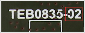
Hardware revision number can be found on the PCB board together with the module model number separated by the dash.
| Scroll Title |
|---|
| anchor | Figure_RV_HRN |
|---|
| title | Board hardware revision number. |
|---|
|
| Scroll Ignore |
|---|
| draw.io Diagram |
|---|
| border | false |
|---|
| viewerToolbar | true |
|---|
| |
|---|
| fitWindow | false |
|---|
| diagramDisplayName | |
|---|
| lbox | true |
|---|
| revision | 4 |
|---|
| diagramName | TEB0835_RV_HRN |
|---|
| simpleViewer | false |
|---|
| width | 200 |
|---|
| links | auto |
|---|
| tbstyle | hidden |
|---|
| diagramWidth | 201 |
|---|
|
|
| Scroll Only |
|---|
|
|
Document Change History
| Page properties |
|---|
|
- Note this list must be only updated, if the document is online on public doc!
- It's semi automatically, so do following
Add new row below first Copy "Page Information Macro(date)" Macro-Preview, Metadata Version number, Author Name and description to the empty row. Important Revision number must be the same as the Wiki document revision number Update Metadata = "Page Information Macro (current-version)" Preview+1 and add Author and change description. --> this point is will be deleted on newer pdf export template - Metadata is only used of compatibility of older exports
|
| Scroll Title |
|---|
| anchor | Table_RH_DCH |
|---|
| title | Document change history. |
|---|
|
| Scroll Table Layout |
|---|
| orientation | portrait |
|---|
| sortDirection | ASC |
|---|
| repeatTableHeaders | default |
|---|
| style | |
|---|
| widths | |
|---|
| sortByColumn | 1 |
|---|
| sortEnabled | false |
|---|
| cellHighlighting | true |
|---|
|
| Date | Revision | Contributor | Description |
|---|
| Page info |
|---|
| infoType | Modified date |
|---|
| dateFormat | yyyy-MM-dd |
|---|
| type | Flat |
|---|
|
| | Page info |
|---|
| infoType | Current version |
|---|
| prefix | v. |
|---|
| type | Flat |
|---|
| showVersions | false |
|---|
|
| | Page info |
|---|
| infoType | Modified by |
|---|
| type | Flat |
|---|
| showVersions | false |
|---|
|
| | | 2023-01-17 | v.54 | Kerstin Möller | | | 2020-12-21 | v.51 | Pedram Babakhani | | -- | all | | Page info |
|---|
| infoType | Modified users |
|---|
| type | Flat |
|---|
| showVersions | false |
|---|
|
| |
|
Disclaimer
| Include Page |
|---|
| IN:Legal Notices |
|---|
| IN:Legal Notices |
|---|
|