Page History
...
Affected Product | Changes | Replacement |
|---|---|---|
| TE0703-06 | #2...# | TE0703-07 |
| TE0703-06-D | #1...# | TE0703-07-D |
Changes
#1
...
Removed VG96 connector from BOM.
Type: Schematic BOM Change
Reason: Follow USB specificationImprove manufacturing process.
Impact: Changed micro USB type B receptable to mirco USB type AB receptable and mechanical component size. Reduced current capability.
...
Connector not longer available within product. If needed, connector needs to be ordered separately.
#2 Changed DCDC (U3) from EN6347QI to MPM3860GQW-Z and adapted power circuit.
Type: Schematic Change
Reason: EOL of Component.
Impact: None. Increased current output capability. Minor changes in electrical characteristics.
...
#3 Changed Load Switch
...
(Q1) from TPS27081ADDCR to Load Switch MP5077GG-Z and adapted circuit.
Type: Schematic Change
Reason: BOM Optimization.
Impact: None. Increased current output capability. Minor changes in electrical characteristics.
...
.
#4 Named enable signal for Load Switch (Q1) to "EN_3.3V_SD".
Type: Schematic Change
Reason: Improve signal identification.
Impact: None.
#5 Changed clock (U6) from SiT8008AI-73-XXS-12.000000E
...
to SiT8008BI-73-XXS-12.000000E.
Type: Schematic Change
Reason: Use new clock revision.
Impact: None.
...
.
#6 Changed USB connector (J12) from 629105150521 to 629105150921.
Type: Schematic Change
Reason: Follow USB specification.
Impact: Changed micro USB type B receptable to micro USB type AB receptable and mechanical component size. Reduced current capability.
#7 Changed SD Card connector (J3) from 504077-1891
...
to MEM2052-00-195-00-A.
Type: Schematic Change
Reason: EOL of Component.
Impact: Mechanical component size increased and push/pull changed to push/push.
Changes
#1
Type:
Reason:
Impact:
Changes
#1
Type:
Reason:
Impact:
Changes
#1
Type:
Reason:
Impact:
Changes
#1
Type:
Reason:
.
#8 Changed pin header (J7) from two pins to three pins and added jumper (J20).
Type: Schematic Change
Reason: Improve manufacturing process.
Impact: None.
#9 Added pull-up resistor (R43) for signal "USB_OC".
Type: Schematic Change
Reason: Enable external pull-up option.
Impact: Firmware reflects it but custom firmware needs to be updated by customer.
#10 Added additional decoupling capacitors C55, C57...C65.
Type: Schematic Change
Reason: Improve decoupling.
Impact: None.
#11 Added testpoints (TP1...TP30).
Type: PCB Change
Reason: Improve voltage monitoring.
Impact: None.
#12 Changed voltage rating for 1 µF capacitors from 6.3 V to 16 V.
Type: Schematic Change
Reason: BOM Optimization.
Impact: None.
#13 Changed voltage rating for 47 µF capacitors from 6.3 V to 10 V and size from 1206 to 0805.
Type: Schematic Change
Reason: BOM Optimization.
Impact: None.
#14 Changed tolerance for 22 µF capacitors from 10 % to 20 % and size from 1206 to 0805.
Type: Schematic Change
Reason: BOM Optimization.
Impact: None.
#15 Changed resistance for 10 kOhm resistors to 12 kOhm.
Type: Schematic Change
Reason: BOM Optimization.
Impact: None.
#16 Changed resistance for 4.7 kOhm resistors (R17...R20) to 5.1 kOhm.
Type: Schematic Change
Reason: BOM Optimization.
Impact: None.
#17 Changed fiducials to standard fiducial type.
Type: Schematic Change
Reason: Use standard fiducials.
Impact: None.
#18 Removed serial number S/N.
Type: Schematic Change
Reason: EOL of Component.
Impact: None.
#19 Added UKCA logo.
Type: PCB Change
Reason: Requiered for export to UK.
Impact: None.
#20 Changed address on silkscreen.
Type: PCB Change
Reason: Updated contact information.
Impact: None.
#21 Updated components from library.
Type: Schematic Change
Reason: Use latest component data.
Impact: None.
#22 Updated legal notices, revision history, block and power diagram. Updated page count and order.
Type: Documentation Update
Reason: Documentation improvement.
Impact: None.Impact:
| Scroll Pagebreak |
|---|
Method of Identification
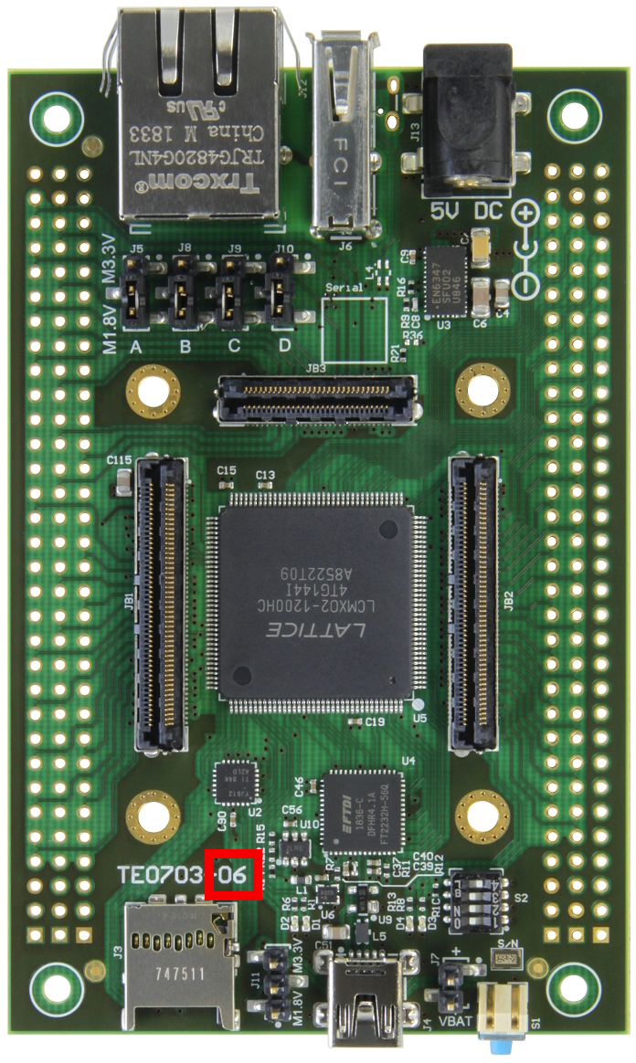
The revision number is shown on the top side of the PCB. Revision number position changes between REV06 and REV07 on top side of the PCB.
Production Shipment Schedule
From XXXXX, after old stock is goneThis change takes place with immediate effect. If the new revision is not suitable for your application and still the former revision of the board is needed, please contact us.
...
Contact Information
If you have any questions related to this PCN, please contact Trenz Electronics Technical Support at
- forum.trenz-electronic.de
- wiki.trenz-electronic.de
- support%trenz-electronic.de (subject = PCN-JJJJMMDD20230705)
phone
national calls: 05741 3200-0
international calls: 0049 5741 3200-0
Disclaimer
Any projected dates in this PCN are based on the most current product information at the time this PCN is being issued, but they may change due to unforeseen circumstances. For the latest schedule and any other information, please contact your local Trenz Electronic sales office, technical support or local distributor.
...
Overview
Content Tools