Page History
...
| Scroll pdf ignore | ||||
|---|---|---|---|---|
Table of Contents
|
Overview
| Scroll Only (inline) |
|---|
Online version of this manual and other related documents can be found at Refer to https://shop.trenz-electronic.de/de/Download/?path=Trenz_Electronic/TE0711 for online version of this manual and the rest of available documentation. |
Trenz Electronic TE0711 is an industrial-grade FPGA module integrating a Xilinx Artix-7 FPGA, 32 MByte Quad SPI Flash memory for configuration and operation and powerful switchswitching-mode power supplies for all on-board voltages. A large number of Numerous configurable I/O's is are provided via rugged high-speed stacking strips. All modules in 4 x 5 cm form factor are mechanically compatible. All this on a tiny footprint, smaller than a credit card
...
size at
...
very competitive price. All Trenz Electronic SoM's in 4 x 5 cm form factor follow the same mechanical design rules, thus they are interchangeable.
Block Diagram

Figure 1: TE0711-01 Block Diagramblock diagram.
Main Components
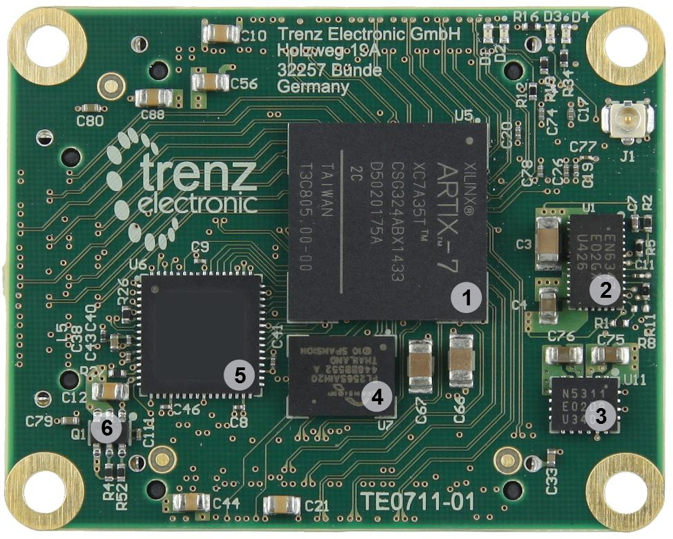
Figure 2: TE0711 (REV 01).
- Artix-7 (15T to 100T) FPGA
- EN6347QI voltage Regulator 1.0V
- EN5311QI voltage Regulator 1.8V
- S25FL256S 32 Mbyte MByte Quad SPI Flash memory
- Dual USB to UART/FIFO Bridge (FT2232H)
- TPS27082L load switch for 3.3V voltage level
- B2B connector JM1 (0,40 mm Razor Beam™ High Speed Hermaphroditic Terminal/Socket Strip (LSHM-150))
- B2B connector JM2 (0,40 mm Razor Beam™ High Speed Hermaphroditic Terminal/Socket Strip (LSHM-150))
- B2B connector JM3 (0,40 mm Razor Beam™ High Speed Hermaphroditic Terminal/Socket Strip (LSHM-150))
- System Controller CPLD (Lattice LCMXO2-256HC): 256 Macrocell CPLD
- SiT8008AI 100 MHz reference clock (connected to FPGA bank 14)
- SiT8008AI 12 MHz reference clock (connected to USB to UART/FIFO Bridge)
- EEPROM (configuration data for USB to UART/FIFO Bridge)
- TPS3805H33 voltage detector for generating "Power OK"-signal indicating successful power-on-sequencing
...
Initial Delivery State
| Storage device nameComponent | Content | Notes |
|---|---|---|
SPI Flash OTP Area | Empty, not programmed | Except serial number programmed by flash vendor. |
SPI Flash Quad Enable bit | Programmed | - |
SPI Flash main array | Demo design | - |
EFUSE USER | Not programmed | - |
EFUSE Security | Not programmed | - |
Table 1: Initial delivery state
...
I/O signals connected to the FPGA's I/O banks and B2B connector:
| Bank | Type | B2B Connector | I/O Signal Count | Voltage | Notes |
|---|---|---|---|---|---|
0 | HR | - | - | 3.3V | Configuration bank |
14 | HR | JM1 |
JM2 | 8 I/O |
pins |
18 I/O |
pins, (9 LVDS |
pairs possible) | 3.3V | HR |
banks support voltages from 1.2V to 3.3V |
. See |
Xilinx Artix-7 datasheet (DS181) for |
voltage |
ranges. | |||
15 | HR | JM1 | 48 I/O |
pins 24 LVDS |
pairs possible |
User |
| As above. | |||
16 | HR | JM1 | 6 I/O |
pins 3 LVDS |
pairs possible | 1.8V |
| As above. | ||
| 34 | HR | JM1 |
JM3 | 48 I/O |
pins 24 LVDS |
pairs possible |
| User |
| As above. | |||
| 35 | HR | JM2 | 50 I/O |
pins 24 LVDS |
pairs possible |
| User |
| As above. |
Table 2: Voltage Voltage ranges and pin-outs of available logic banks of the FPGA.
Please use Master Pinout Pin-out Table table as primary reference for the pin mapping information.
...
| JTAG Signal | B2B Connector |
|---|---|
| TCK | JM2-99 |
| TDI | JM2-95 |
| TDO | JM2-97 |
| TMS | JM2-93 |
| JTAGSEL | JM1-89 |
Table 3Table 3: Pin-mapping of JTAG Interface on B2B connector
| Note |
|---|
| Select by JTAGSEL pin on B2B connector JM1 is used to control which physical device is accessible via JTAG interface. If this pin is set to low or left open, JTAG interface is enabled for Xilinx Artix-7 FPGA, if set to high, JTAG interface for System Controller CPLD will be enabled. The use of Xilinx legacy development tools (ISE, iMPACT) is not recommended. iMPACT does not recognize any Xilinx Artix-7 below A100T model. |
System Controller I/O Pins
...
Overview
Content Tools