Page History
...
Trenz Electronic TE0711 is an industrial-grade FPGA module integrating a Xilinx Artix-7 FPGA, 32 MByte Quad SPI Flash memory for configuration and operation and powerful switching-mode power supplies for all on-board voltages. Numerous configurable I/O's are provided via rugged high-speed strips. All this on a tiny footprint, smaller than a credit card size at very competitive price. All Trenz Electronic SoM's in 4 x 5 cm form factor are mechanically compatible.
Block Diagram
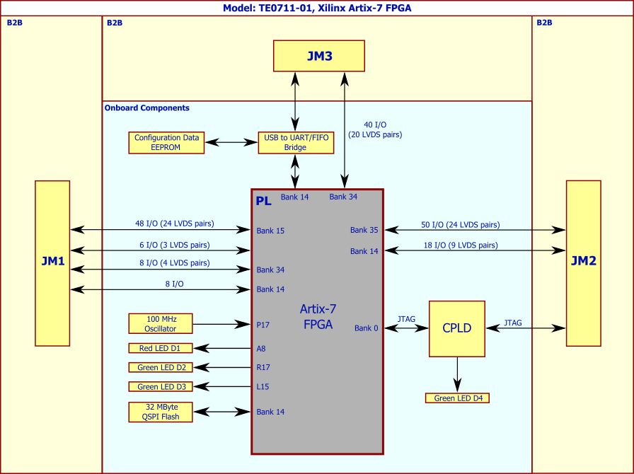
Figure 1: TE0711-01 block diagram.
...
- Xilinx Artix-7 FPGA
- EN6347QI voltage regulator 1.0V
- EN5311QI voltage regulator 1.8V
- 32 MByte Quad SPI Flash memory
- Dual USB to UART/FIFO Bridge (FT2232H)
- TPS27082L load switch for 3.3V voltage level
- B2B connector Samtec Razor Beam™ LSHM-150, JM1
- B2B connector Samtec Razor Beam™ LSHM-150, JM2
- B2B connector Samtec Razor Beam™ LSHM-130, JM3
- System Controller CPLD
- SiT8008AI 100 MHz reference clock (connected to FPGA bank 14)
- SiT8008AI 12 MHz reference clock (connected to USB to UART/FIFO Bridge)
- EEPROM (configuration data for USB to UART/FIFO Bridge)
- TPS3805H33 voltage detector for generating "Power OK"-signal indicating successful power-on-sequencing
...
I/O signals connected to the FPGA's I/O banks and B2B connector:
| Bank | Type | B2B Connector | I/O Signal Count | Voltage | Notes |
|---|
0
HR
-
14 | HR | JM1 JM2 | 8 I/O pins 18 I/O pins, |
(9 LVDS pairs |
) | 3.3V | HR banks support voltages from 1.2V to 3.3V. See Xilinx Artix-7 datasheet (DS181) for voltage ranges. | |
15 | HR | JM1 | 48 I/O pins 24 LVDS pairs |
User | As above. | ||
16 | HR | JM1 | 6 I/O pins 3 LVDS pairs |
1.8V | As above. | ||
| 34 | HR | JM1 JM3 | 48 I/O pins 24 LVDS pairs |
| User | As above. | ||
| 35 | HR | JM2 | 50 I/O pins 24 LVDS pairs |
| User | As above. |
Table 2: Voltage ranges and pin-outs of available logic banks of the FPGA.
...
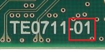
Hardware revision number is printed on the PCB board together with the module model number separated by the dash.
Document Change History
| Date | Revision | Contributors | Description |
|---|---|---|---|
| 2017-01-27 | Jan Kumann | New block diagram. | |
| 2017-01-01 | V10 | Ali Naseri, Thorsten Trenz, Jan Kumann | TRM revision. |
| 2015-06-05 |
| V0.1 | Antti Lukats | Initial version. |
Disclaimer
| Include Page | ||||
|---|---|---|---|---|
|
Overview
Content Tools