Page History
...
| Scroll Only (inline) |
|---|
Refer to https://shopwiki.trenz-electronic.de/dedisplay/Download/?path=Trenz_Electronic/TE0725PD/TE0725+TRM for downloadableonline version of this manual and the rest of available documentation of the product. |
The Trenz Electronic TE0725 is a low cost small-sized FPGA module integrating a Xilinx Artix-7 (15-100T) and 32 MByte Flash memory for configuration and operation.
Key Features
Xilinx Artix-7 XC7A35T (A15 to A100T)
Commercial Temperature Grade (Industrial on Request)
32 MByte Flash Memory
2 x 50 Pin Headers with 2,54mm Pitch, Ideal for Breadboard Use
- 87 IOs (42 + 42 + 3)
- 100 MHz System Clock
- I2C EEPROM
3.3V Single Power Supply with On-Board Voltage Regulators
Size 73 x 35 mm
JTAG/UART Connector
2 LED's
- Optional HyperRAM (8 to 32 MByte)
- Optional POF Fiber Optical Adapter (125/250 Mbps)
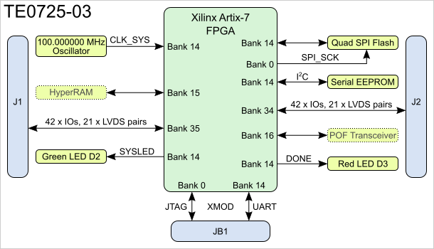
Block Diagram
| Page break |
|---|
Main Components
...
- Xilinx Artix-7 FPGA, U1
- 32-MByte Flash Memorymemory, U7
- Enpirion EN6347 4A PowerSoC DC-DC Step Down Converterstep down converter, U10
- Enpirion EN5311 1A PowerSoC Synchronous Buck Regulator With Integrated Inductorsynchronous buck regulator with integrated inductor, U11
- POF Transceiver transceiver placeholder, U8
- 50-pin placeholder for breadboard connector, J1
- 50-pin placeholder for breadboard connector, J2
- JTAG/UART connector, JB1
- Green LED D2(SYSLED) and Red red LED D3(DONE)
- 16K x 8 (128-Kbit) Serial serial EEPROM, U2
- Low-Noisenoise, High high PSRR, RF, 200-mA Low-Dropout Linear Regulatorlow-dropout linear regulator, U9
- Ultralow Supply-Current Voltage Monitor With Optional WatchdogUltra-low supply-current voltage monitor with optional watchdog, U6
- Cypress S27KS0641 64-Mbit (8-MByte) HyperRAM™ Selfself-Refresh refresh DRAM, U4
Key Features
Xilinx Artix-7 XC7A35T (A15 to A100T)
Commercial Temperature Grade (Industrial on Request)
32 MByte Flash Memory
2 x 50 Pin Headers with 2,54mm Pitch, Ideal for Breadboard Use
- 87 IOs (42 + 42 + 3)
- 100 MHz System Clock
- I2C EEPROM
3.3V Single Power Supply with On-Board Voltage Regulators
Size 73 x 35 mm
JTAG/UART Connector
2 LED's
- Optional HyperRAM (8 to 32 MByte)
- Optional POF Fiber Optical Adapter (125/250 Mbps)
Signals, Interfaces and Pins
...
| Bank | VCCIO | B2B I/O | Notes |
|---|---|---|---|
| 0 | 3.3V | 0 | JTAG |
| 14 | 3.3V | 0 (3) | 3 I/O in XMOD-JTAG - for use as UART |
| 15 | 1.8V | 0 | used for optional hyper RAM |
| 16 | 2.5V | 0 | used for optional optical fiber transceiver |
| 34 | User select | 42 | 0R resistor option to select 3.3V |
| 35 | User select | 42 | 0R resistor option to select 3.3V |
...

...
AFBR-59F2Z
...
JTAG Interface
JTAG access to the Xilinx Artix-7 device is provided through connector JB1.
...
Connector JB1 (2 x 6 pin Header) is directly compatible to with XMOD JTAG Adapter TE0790. This adapter can be inserted from top onto the TE0725, if JB1 is fitted with male pin header. Optionally JB1 can be fitted with pin header from bottom, in that case the JTAG cable connector must be on the base board.
...
When using XMOD-JTAG please check the switch settings on XMOD to be sure the power and I/O reference are supplied correctly. TE0790 can be in some cases used to power up TE0725, however this is not recommended. TE0790-01 can not supply enough power for TE0725 (LED may blink but the module is not operating properly, especially in case of larger and more sophisticated designs).
POF Transceiver
| Model | Bitrate MB/s | Notes |
|---|---|---|
AFBR-59F2Z | 250 |
On-board LED's
| LED | Color | FPGA | Notes |
|---|---|---|---|
| D2 | Green | M16 | |
| D3 | Red | DONE | Active low |
...
Technical Specifications
Absolute Maximum Ratings
Parameter | Min | Max | Units |
|---|
| Reference document |
|---|
3.3V supply voltage | -0.1 | 3.6 | V |
| HR I/O |
| banks supply voltage (VCCO) | -0.5 | 3.6 | V |
| Xilinx datasheet DS181 |
| HR I/O banks input voltage |
| -0.4 | VCCO |
Voltage on Module JTAG pins
-0.4
V
| + 0.55 | V |
| Xilinx datasheet DS181 |
Storage Temperature | -40 | +85 | °C |
Recommended Operating Conditions
| Parameter | Min | Max | Units |
|---|
| Reference document | ||||
|---|---|---|---|---|
| VIN supply voltage | 3.135 | 3.45 | V |
| HR I/O banks supply voltage (VCCO) | 1.14 | 3.465 | V |
| Xilinx datasheet DS181 |
| HR I/O banks input voltage |
| -0.20 | VCCO + 0.20 | V |
| Xilinx datasheet DS181 |
3.3V CONFIG Bank Option
| Operating Temperature | 0 | +85 | °C |
| Note |
|---|
| Please check Xilinx datasheet DS181 for complete list of absolute maximum and recommended operating ratings for the Artix-7 device (DS181). |
| Page break |
|---|
Physical Dimensions
...
Overview
Content Tools