Page History
...
Figure 1: TEBA0841-01 Block Diagram
Main Components
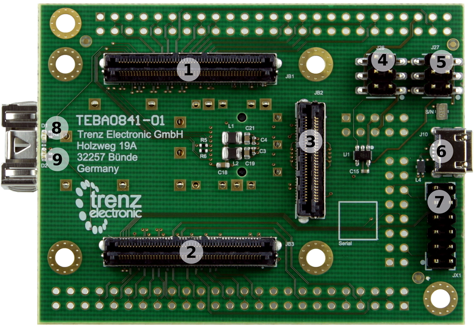
Figure 2: 4 x 5 SoM carrier board TEBA0841-01
...
The pin-assignment of the SFP connector is in detail as fellows:
| SFP+ pin | SFP+ pin netnameSchematic Name | B2B | Note |
|---|---|---|---|
| Transmit Data + (pin 18) | MGT_TX3_P | JB2-26 | - |
| Transmit Data - (pin 19) | MGT_TX3_N | JB2-28 | - |
| Receive Data + (pin 13) | MGT_RX3_P | JB2-25 | - |
| Receive Data - (pin 12) | MGT_RX3_N | JB2-27 | - |
| Receive Fault (pin 2) | MIO10 | JB1-96 | - |
| Receive disable (pin 3) | not connected | - | - |
| MOD-DEF2 (pin 4) | MIO13 | JB1-98 | 3.3V pull-up, (usable I²C SDA/SCL-line) |
| MOD-DEF1 (pin 5) | MIO12 | JB1-100 | 3.3V pull-up, (usable I²C SDA/SCL-line) |
| MOD-DEF0 (pin 6) | MIO11 | JB1-94 | - |
| RS0 (pin 7) | not connected | - | - |
| LOS (pin 8) | MIO0 | JB1-88 | - |
| RS1 (pin 9) | not connected | - | - |
...
| MGT-lane | B2B TX diff-pair | B2B RX diff-pair | B2B - pins bridged |
|---|---|---|---|
| MGT-lane 0 | JB2-8 (MGT_TX0_N) JB2-10 (MGT_TX0_P) | JB2-7 (MGT_RX0_N) JB2-9 (MGT_RX0_P) | JB2-7 to JB2-8 JB2-9 to JB2-10 |
| MGT-lane 1 | JB2-14 (MGT_TX1_N) JB2-16 (MGT_TX1_P) | JB2-13 (MGT_RX1_N) JB2-15 (MGT_RX1_P) | JB2-13 to JB2-14 JB2-15 to JB2-16 |
| MGT-lane 2 | JB2-20 (MGT_TX2_N) JB2-22 (MGT_TX2_P) | JB2-19 (MGT_RX2_N) JB2-21 (MGT_RX2_P) | JB2-19 to JB2-20 JB2-21 to JB2-22 |
| MGT-lane 7 | JB1-3 (MGT_TX7_P) JB1-5 (MGT_TX7_N) | JB1-9 (MGT_RX7_P) JB1-11 (MGT_RX7_N) | JB1-3 to JB1-9 JB1-5 to JB1-11 |
| MGT-lane 6 | JB1-15 (MGT_TX6_P) JB1-17 (MGT_TX6_N) | JB1-21 (MGT_RX6_P) JB1-23 (MGT_RX6_N) | JB1-15 to JB1-21 JB1-17 to JB1-23 |
...
This header has a 'XMOD FTDI JTAG Adapter'-compatible pin-assignment, so the XMOD-FT2232H adapter-board TE0790 can be used in conjunction with the carried board to program the mounted SoM via USB interface.
| JX1 pin | JX1 pin net-nameSchematic Name | B2B | J3 pin | J3 pin net-nameSchematic Name | B2B | |
|---|---|---|---|---|---|---|
| C (pin 4) | TCK | JB3-100 | 4 | TCK | JB3-100 | |
| D (pin 8) | TDO | JB3-98 | 8 | TDO | JB3-98 | |
| F (pin 10) | TDI | JB3-96 | 10 | TDI | JB3-96 | |
| H (pin 12) | TMS | JB3-94 | 12 | TMS | JB3-94 | |
| A (pin 3) | MIO15 | JB1-86 (usable as UART RX/TX-line) | 3 | MIO15 | JB1-86 (usable as UART RX/TX-line) | |
| B (pin 7) | MIO14 | JB1-91 (usable as UART RX/TX-line) | 7 | MIO14 | JB1-91 (usable as UART RX/TX-line) | |
| E (pin 9) | BOOTMODE | JB1-90 (JTAGSELECT) | 9 | BOOTMODE | JB1-90 (JTAGSELECT) | |
| G (pin 11) | RESIN | JB3-17 | 11 | RESIN | JB3-17 | |
| - | - | - | 15 | CLK0_N | JB2-32 (MGT_CLK0_N, decoupling capacitator 100 nF) | |
| - | - | - | 16 | CLK0_P | JB2-34 (MGT_CLK0_P, decoupling capacitator 100 nF) |
...
Two LEDs are present on the TEBB0714 base-board with following functionality:
| LED designatorDesignator | color | Color | Pin Schematic Namepin net-name | B2B -connectorConnector | indicatingIndicating |
|---|---|---|---|---|---|
| D1 | green | MIO9 | JB1-92 | available to user | |
| D2 | red | RLED | JB3-90 | available to user |
Table 4: LED's functionality
Place
...
Holders for
...
Optional Pin-headers
The TEBA0841 base-board has place-holders with solder-pads to mount optional pin-headers capable to access the PL IO-bank pins of the mounted 4 x 5 SoM. With this user interfaces, a large quantity of IO's are also usable as LVDS-pairs and different VCCIO's are available to operate the IO's properly.
...
On the TEBA0841 carrier board the PL IO-bank's supply voltages of the 4x5 SoM (VCCIOA, VCCIOD; see 4x5 Module Integration Guide) are connected to the base-board VCCIO-voltage VCCIOA and VCCIOD, which are selectable between the supply-voltages 1.8V, 2.5V and 3.3V via jumper J26 and J27.
Baseboard Supply Voltages | Base | baseboard supply-voltages | base-board B2B connector-pinsConnector Pins | Standard Assignment standard assignment of PL IO-bank supply-voltagesSupply Voltages on TE 4x5 moduleModule's B2B connectors-pinsConnectors Pins |
|---|---|---|---|---|
| VCCIOA | JB1-10, JB1-12 | VCCIOA (JM1-9, JM1-11) | ||
| VCCIOD | JB2-8, JB2-10 | VCCIOD (JM2-7, JM2-9) |
...
| Note |
|---|
Note: The corresponding PL IO-voltage supply voltages of the 4x5 SoM to the selectable base-board voltage VCCIOA and VCCIOD are depending on the mounted 4x5 SoM and varying in order of the used model. Refer to SoM's schematic to get information about the specific pin-assignment on module's B2B-connectors regarding PL IO-bank supply-voltages and to the 4x5 Module integration Guide for VCCIO voltage options. |
Following table describes how to configure the base-board supply-voltages by jumpers:
baseBase-board supply-voltagesSupply Voltages | VCCIOA | VCCIOD |
|---|---|---|
| 1.8V | J26:1-2 | J27:1-2 |
| 2.5V | J26:3-4 | J27:3-4 |
| 3.3V | J26:5-6 | J27:5-6 |
Table 6: Configuration of base-board supply-voltages via jumpers. Jumper-Notification: 'Jx: 1-2' means pins 1 and 2 are connected, 'Jx: 3-4' means pins 3 and 4 are connected, and so on.
| Note |
|---|
| It is recommended to set and measure the PL IO-bank supply-voltages before mounting of TE 4x5 module to avoid failures and damages to the functionality of the mounted SoM. |
...
Overview
Content Tools