Page History
...
See also Xilinx datasheet DS892 for additional information. User should also check related baseboard documentation when choosing baseboard design for TE0720 module.
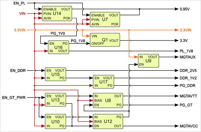
Figure 3: TE0841-01 Power-on sequence.
Power Rails
| Power Rail Name | B2B JM1 Pins | B2B JM2 Pins | Input/Output | Notes |
|---|---|---|---|---|
| VIN | 1, 3, 5 | 2, 4, 6, 8 | Input | Supply voltage. |
| 3.3VIN | 13, 15 | - | Input | Supply voltage. |
| B64_VCO | 9, 11 | - | Input | HR (High Range) bank voltage. |
| B66_VCO | - | 1, 3 | Input | HP (High Performance) bank voltage. |
| B67_VCO | - | 7, 9 | Input | HP (High Performance) bank voltage. |
| B68_VCO | - | 5 | Input | HP (High Performance) bank voltage. |
VBAT_IN | 79 | - | Input | RTC battery supply voltage. |
| 3.3V | - | 10, 12, 91 | Output | Module on-board 3.3V voltage level. |
...
All dimensions are given in millimeters.
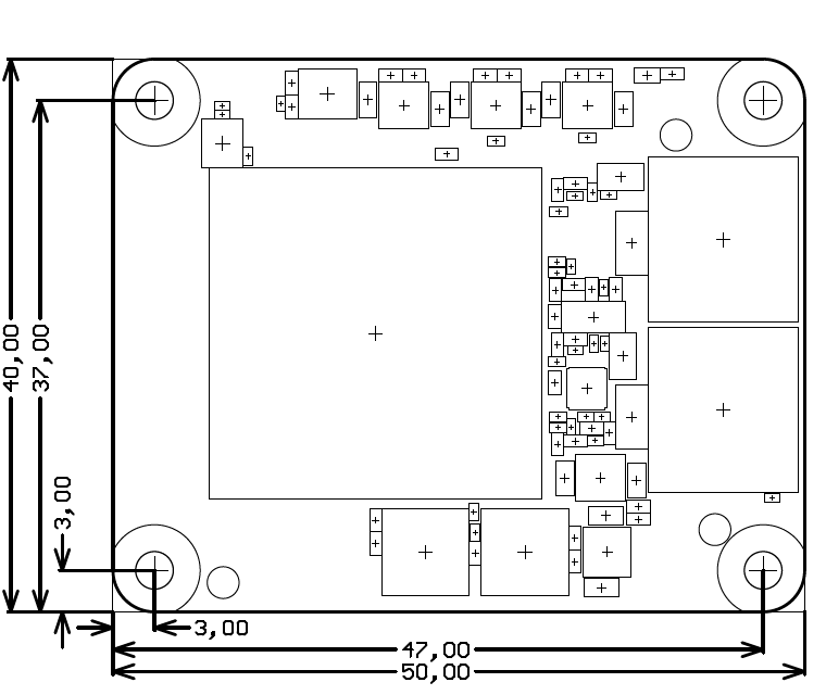
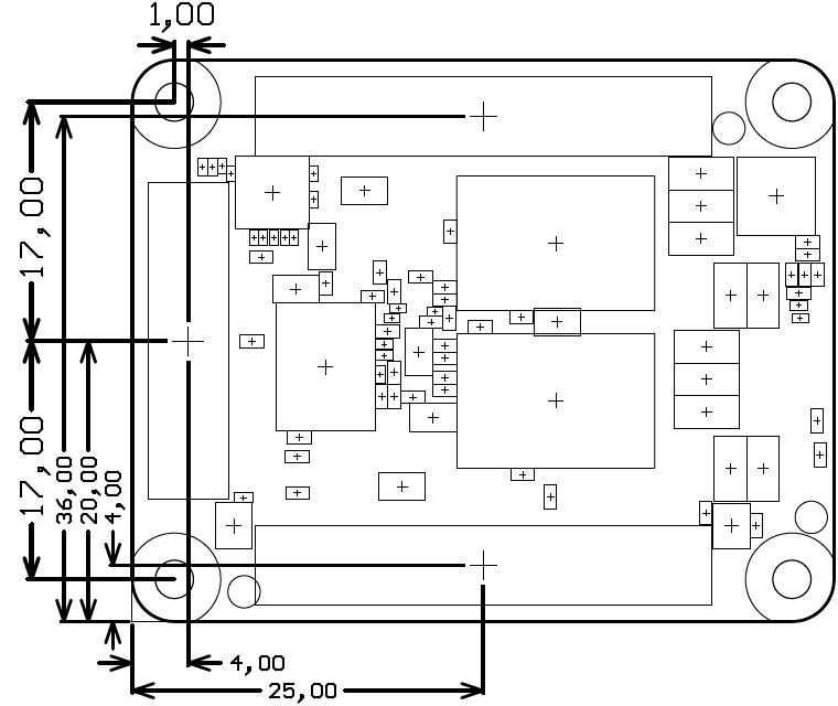
Figure 34: Module physical dimensions.
...
Hardware revision number is printed on the PCB board together with the module model number separated by the dash.
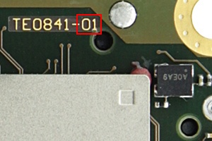
Figure 45: Module hardware revision number.
...
Overview
Content Tools