Page History
...
- 6-pin header J26 for selecting PL-bank I/O voltage
- 6-pin header J27 for selecting XMOD/JTAG VCCIO
- Samtec Razor Beam™ LSHM-150 B2B connector, JM1
- Samtec Razor Beam™ LSHM-150 B2B connector, JM2
- XMOD header, JX1
- Ultra small SMT coaxial connector, J5
- Ultra small SMT coaxial connector, J6
- Ultra small SMT coaxial connector, J7
- Ultra small SMT coaxial connector, J8
- User LED D1 (green)
- User LED D2 (red)
- LED D3 (red) indicating FPGA's 'Programming DONE'-signal
- SFP+ Connector, J1
- 10-pin header solder pads J4 for access to SoM's PL I/O-banks (LVDS - pairs possible)
- 16-pin header solder pads J3, JTAG/UART header ('XMOD FTDI JTAG Adapter'-compatible pin-assignment)
- 50-pin header solder pads J20 for access to SoM's PL I/O-banks (LVDS pairs possible)
- 50-pin header solder pads J17 for access to SoM's PL I/O-banks (LVDS pairs possible)
...
| Connector Designator | Connected to | B2B Connector |
|---|---|---|
| J5 | MGT_TX3_P | JM1-8 |
| J6 | MGT_TX3_N | JM1-10 |
| J7 | MGT_RX3_P | JM1-1 |
| J8 | MGT_RX3_N | JM1-3 |
Table 24: Pin-assignment of the coaxial connectors.
...
The I/O-voltage of the XMOD adapter board with the schematic name 'V_CFG' and pin-name 'VIO' (pin 6) on XMOD header JX1 can be selected via Jumper J27:
V_CFG Value | Jumper J27 Setting | Note |
|---|---|---|
| 1.8V | pins 1-2 connected | Module's output voltage. |
| V_CFG0 | pins 3-4 connected | Internal module |
| VCCIO: 3.3V or 1.8V, depending on TE0714 module configuration. | ||
| 3.3V_OUT | pins 5-6 connected | Module's output voltage. |
Table 78: Setting of reference I/O-voltage XMOD header.
...
| Pin Schematic Name | Header J3 Pin | B2B | Note |
|---|---|---|---|
| TCK | 4 | JM1-90 | - |
| TDO | 8 | JM1-88 | - |
| TDI | 10 | JM1-86 | - |
| TMS | 12 | JM1-92 | - |
| B14_L25 | 3 | JM2-97 | UART-TX (transmit line) |
| B14_L0 | 7 | JM2-99 | UART-RX (receive line) |
| BOOTMODE | 9 | JM2-100 | - |
| PROG_B | 11 | JM1-94 | - |
| XADC_P | 13 | JM1-25 | Analog input differential pair |
| XADC_N | 14 | JM1-27 | |
| CLK0_N | 15 | JM1-4 | AC decoupled on-board (100 nF capacitor) |
| CLK0_P | 16 | JM1-2 |
Table 89: JTAG/UART header J3 signals and connections.
...
| UART Signal Schematic Name | B2B | XMOD Header JX1 | Pin Header J3 | Note |
|---|---|---|---|---|
| B14_L0 | JM2-99 | JX1-7 | J3-7 | UART-RX (receive line) |
| B14_L25 | JM2-97 | JX1-3 | J3-3 | UART-TX (transmit line) |
Table 610: UART interface signals.
QSPI Interface
...
| SD IO Signal Schematic Name | B2B | Pin Header J17 | Note |
|---|---|---|---|
| SPI-DQO | JM2-68 | J17-24 | QSPI data |
| SPI-DQ1 | JM2-71 | J17-27 | QSPI data |
| SPI-DQ2 | JM2-73 | J17-28 | QSPI data |
| SPI-DQ3 | JM2-70 | J17-23 | QSPI data |
| SPI-CLK | JM2-67 | J17-26 | QSPI clock |
| SPI_CS | JM2-69 | J17-25 | QSPI chip select |
Table 711: QSPI interface signals.
On-board Peripherals
...
The on-board LEDs are available to the user and can be used to indicate system status and activities:
| LED Designator | Color | Pin Schematic Name | B2B Connector | Indicating |
|---|---|---|---|---|
| D1 | green | GLED | JM2-26 |
| Available to user. | |||
| D2 | red | RLED | JM2-24 |
| Available to user. | ||||
| D3 | red | DONE | JM1-96 | FPGA |
| module programmed properly. |
Figure 1112: On-board LEDs
VCCIO Selection Jumper
On the TEBB0714 Carrier Board the PL-bank I/O voltage (schematic name 'VCCIO34') can be selected by the jumper J26.
VCCIO34 Value | Jumper J26 Setting | Note |
|---|---|---|
| 1.8V | pins 1-2 connected | Module's output voltage. |
| 2.5V | pins 3-4 connected | Voltage generated by on-board LDO U1. |
| 3.3V_OUT | pins 5-6 connected | Module's output voltage. |
Table 1213: Base-board PL-bank I/O voltage setting.
...
Following diagram shows the distribution of the external input voltage of nominal 3.3V to the components:
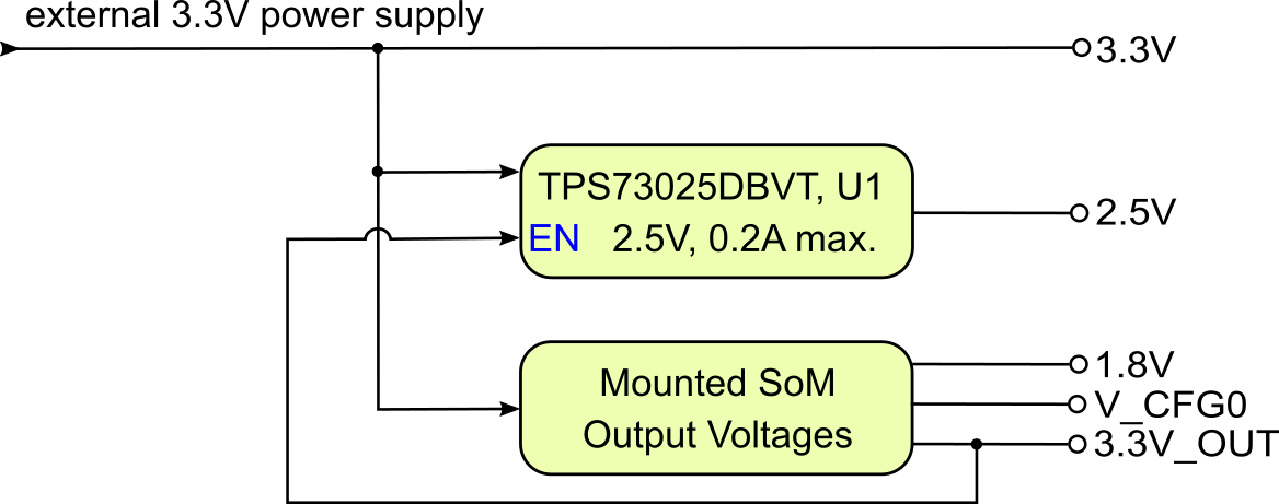
Figure 43: Board power distribution diagram.
...
| Module Connector (B2B) Designator | VCC / VCCIO | Direction | Pins | Notes | ||
|---|---|---|---|---|---|---|
| JB1JM1 | 3.3V | Out | 2, 4, 6, 14, 1697, 99 | 3.3V module supply voltage | ||
| 3.3V_OUT | In | 83 | 3.3V module output voltage | |||
| VCCIO34VCCIOA | Out | 10, 1261 | PL IO-bank VCCIO | |||
| JM2 | M11. | 8VOUT8V | In | 4018 | 1.8V module output voltage | JB2|
| 3.3V_OUT | InOut | 9, 1154 | 3.3V module output voltage | |||
| 3.3V | Out | 1, 3, 5, 7 | 3.3V module supply voltage | |||
| VCCIOD | Out | 8, 10 | PL IO-bank VCCIO | |||
| JB3 | USB-VBUS | Out | 56 | USB Host supply voltage | ||
| V_CFG0 | In | 53 | Internal module VCCIO: 3.3V or 1.8V |
Table 16: Power pin description of B2B module connector.
...
| On-board Pin Header Designator | VCC / VCCIO | Direction | Pins | Notes |
|---|---|---|---|---|
| J17 | 3.3V | In / Out | 5, 4846 | 3.3V external supply voltage |
| VCCIODV_CFG | In / Out | 6, 45 | PL IO-bank VCCIO, depends on Jumper jumper 27 settings | |
| J20 | 3.3V | In / Out | 5, 4846 | 3.3V external supply voltage |
| VCCIOAVCCIO34 | In / Out | 6, 45 | PL IO-bank VCCIO, depends on Jumper settings |
...
| Jumper / Header Designator | VCC / VCCIO | Direction | Pins | Notes | ||
|---|---|---|---|---|---|---|
| J26 | VCCIOAVCCIO34 | In | 21, 43, 65 | - | ||
| M11.8VOUT8V | Out | 12 | - | |||
| 2.5V | Out | 34 | - | |||
| 3.3V_OUT | Out | 56 | - | |||
| J27 | VCCIODV_CFG | In | 21, | 43, | 65 | - |
| M11.8VOUT8V | Out | 12 | -2.5V | |||
| V_CFG0 | Out | 34 | - | |||
| 3.3V_OUT | Out5 | - | ||||
| J4 | 3.3V | Out | 5 | - | ||
| M1.8VOUT | Out | 6 | - |
Table 18: Power Pin description of VCCIO selection jumper pin header.
...
Table 19: Power pin description of peripheral connector.
| XMOD JTAG/UART Header Designator | VCC / VCCIO | Direction | Pins | Notes |
|---|---|---|---|---|
| JX1 (XMOD) | 3.3V | Out | 5 | connectedConnected to 3.3V external supply voltage |
| VIO | Out | 6 | ||
| VIO | Out | 6 | Connected to 'V_CFG', depends on jumper 27 settings | |
| J3 | 3.3V | Out | 5 | connectedConnected to 3.3V external supply voltage |
| 3.3VV_CFG | Out | 6 | VCCIO, depends on jumper 27 settings |
Table 19Table 20: Power pin description of XMOD/JTAG Connector.
...
| Parameter | Min | Max | Units | Notes |
|---|---|---|---|---|
Vin supply voltage | 3.135 | 3.465 | V | 3.3V supply-voltage ± 5% |
Storage Temperature | -5540 | 10585 | °C | Molex 74441-0001 Product SpecificationWL-SMCW SMD chip LED data sheet |
Table 2120: Board absolute maximum ratings.
...
| Parameter | Min | Max | Units | Notes |
|---|---|---|---|---|
| Vin supply voltage | 3.135 | 3.465 | V | - |
| Operating temperature | -40 | +85 | °C | Molex 74441-0001 Product Specification |
Table 2221: Module recommended operating conditions.
...
Physical Dimensions
Board size: PCB 56.47 mm × 75 mm46mm × 75mm. Notice that some parts the are hanging slightly over the edge of the PCB like the mini USB-jacks and the SFP+ connector, which determine the total physical dimensions of the carrier board. Please download the assembly diagram for exact numbers.
Mating height of the module with standard connectors: 8mm
PCB thickness: ca. 1.65mm
Highest part on the PCB is the SFP+ connector, which has an approximately 11.3 mm overall hight. Please download the step model for exact numbers.
The dimensions are given in mm and mil (milli inch).
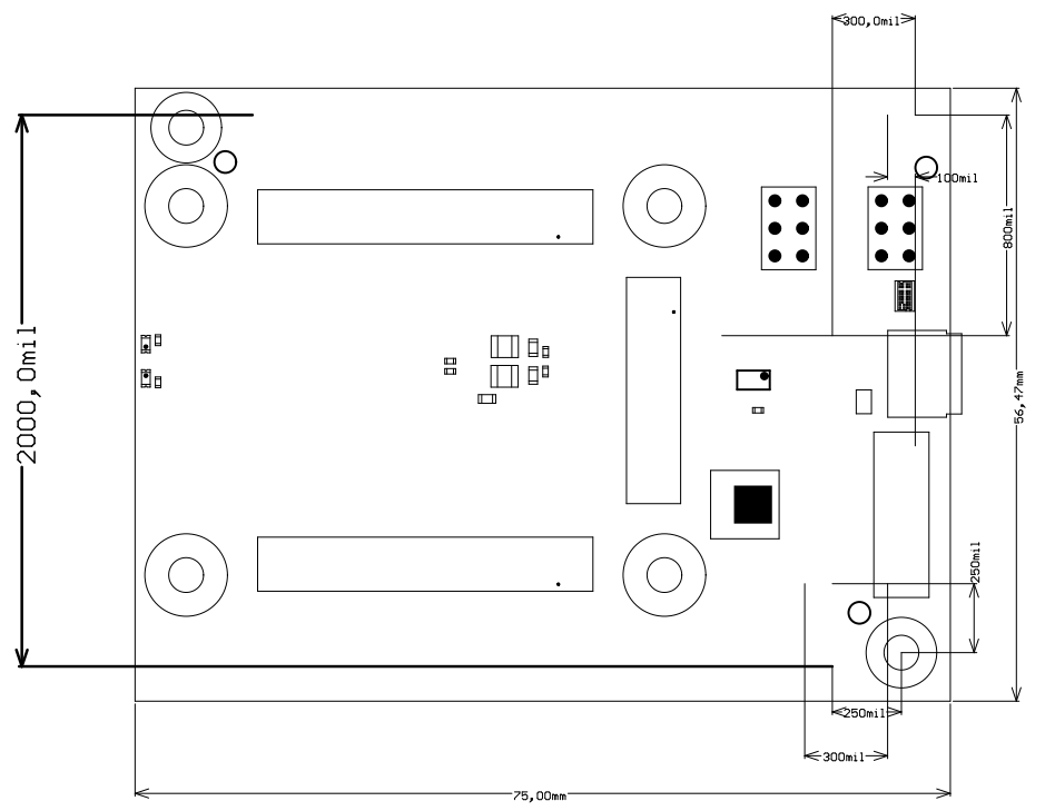
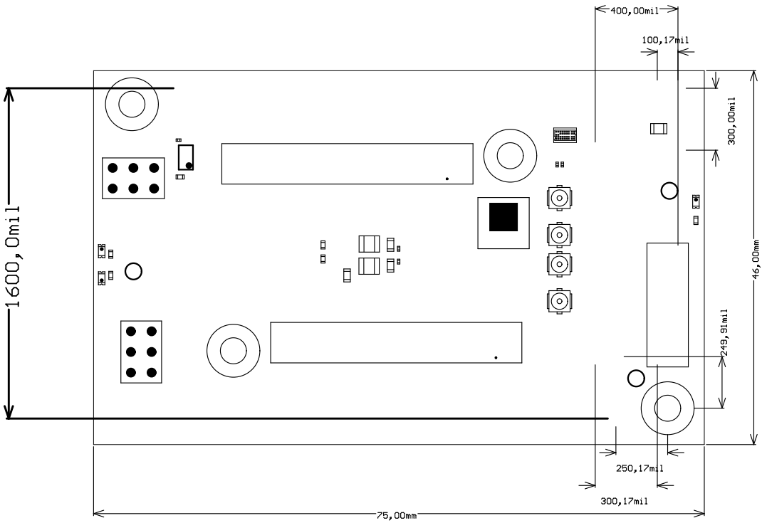
Figure 54: Board physical dimensions drawing.
...
| Date | Revision | Notes | PCN | Documentation Link |
|---|---|---|---|---|
| - | 01 |
| - | TEBB0714-01 |
Table 2322: Module hardware revision history.
Hardware revision number can be found on the PCB board together with the module model number separated by the dash.
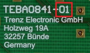
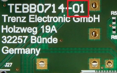
Figure 65: Board hardware revision number.
...
Date | Revision | Contributors | Description | ||||||||
|---|---|---|---|---|---|---|---|---|---|---|---|
| Ali Naseri, Jan Kumann |
|
Table 2423: Document change history.
...
Overview
Content Tools