Page History
...
There is no specific or special power-on sequence, single power source is needed as 3.3V as power supply voltage.
Voltage Monitor Circuit
The voltages 1.0V (core voltage) and 3.3V are monitored by the voltage monitor circuit U6, which generates the POR_B reset signal at power-on. A manual reset is also possible by driving the connector pin P1-10 ('NRST') to GND. Leave this pin unconnected or connect to VDD (3.3V) when unused.
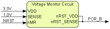
Figure 5: Voltage monitor circuit
Power Rails
Power Rail Name | J1 Pins | J2 Pins | J3 Pins | P1 Pin | P2 Pin | Direction | Notes |
|---|---|---|---|---|---|---|---|
| 3.3V | 5, 6 | 5, 6 | 5, 6 | 9 | 9 | Input / Output | 3.3V power supply voltage |
Table 13: Board power rails
Bank Voltages
Bank | Bank I/O Voltage VCCO | Voltage Range |
|---|---|---|
| 0 (config) | 3.3V | fixed |
| 500 (MIO) | 3.3V | fixed |
| 501 (MIO) | 3.3V | fixed |
| 34 (HR) | 3.3V | fixed |
| 35 (HR) | 3.3V | fixed |
Table 14: Board bank voltages
Variants Currently in Production
| Board Variant | Xilinx Zynq SoC | ARM Cores | PL Cells | LUTs | Flip-Flops | Block RAM | DSP Slices | Zynq SoC Operating Temp. | Temp. Range |
|---|---|---|---|---|---|---|---|---|---|
| TE0722-02I | XC7Z010-1CLG225I | A9+ Dual-core | 28K | 17,6K | 35,2K | 2.1 MBytes | 80 | –40°C to +100°C | Industrial |
| TE0722-02 | XC7Z010-1CLG225C | A9+ Dual-core | 28K | 17,6K | 35,2K | 2.1 MBytes | 80 | 0°C to +85°C | Commercial |
| TE0722-02-07S-1C | XC7Z007S-1CLG225C | A9+ Single-core | 23K | 14,4K | 28,8K | 1.8 MBytes | 66 | 0°C to +85°C | Commercial |
Table 1315: Board variants
Technical Specifications
...
Parameter | Min | Max | Units | Reference Document |
|---|---|---|---|---|
3.3 supply voltage | -0.3 | 3.6 | V | EN5311QI datasheet / Xilinx datasheet DS187 |
| HR PL I/O banks input voltage (VCCIO single ended) | -0.4 | VCCO + 0.55 | V | Xilinx datasheet DS187 (VCCO 3.3V nominal) |
Storage temperature | -40 | +85 | °C | Silicon Labs Si1141/42/43 datasheet. |
Table 1416: Board absolute maximum ratings
...
| Parameter | Min | Max | Units | Reference Document |
|---|---|---|---|---|
| 3.3 supply voltage | 3.3 | 3.465 | V | Xilinx datasheet DS187 |
| HR PL I/O banks input voltage (VCCIO single ended) | -0.20 | VCCO + 0.20 | V | Xilinx datasheet DS187 (VCCO 3.3V nominal) |
Operating Temperature Commercial | 0 | +85 | °C | Xilinx datasheet DS190 |
Operating Temperature Industrial | -40 | +85 | Xilinx datasheet DS190 |
Table 1517: Board recommended operating condition
...
All dimensions are given in millimeters.
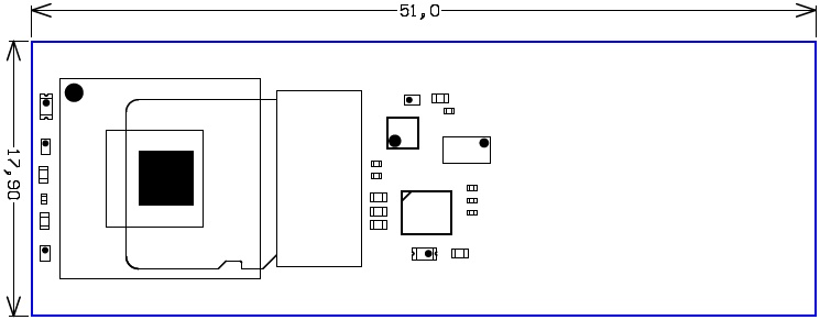
Figure 56: Board physical dimensions
...
| Date | Revision | Notes | PCN | Documentation Link |
|---|---|---|---|---|
| - | 02 | - | - | TE0722-02 |
| - | 01 | First production release | - | - |
Table 1118: Board hardware revision history
Hardware revision number is printed on the PCB board together with the module model number separated by the dash.
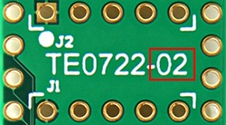
Figure 67: TE0722 module hardware revision number
...
Date | Revision | Contributors | Description | ||||||||
|---|---|---|---|---|---|---|---|---|---|---|---|
| Ali Naseri, Jan Kumann |
|
Table 1219: Document change history
Disclaimer
...
Overview
Content Tools