Page History
...
| Scroll Only (inline) |
|---|
Refer to http://trenz.org/te0725LP-info for online version of this manual and the rest of available documentation of the product.
|
Key Features
Xilinx Artix-7 XC7A100T FPGA
32 MByte QSPI Flash memory
2 x 50-pin headers with 2,54mm pitch, ideal for breadboard use
- 92 x GPIOs (42 + 42 + 8)
- 25.000000 MHz system clock
- 128 KBit (16 KByte) I2C EEPROM
3.3V single power supply with on-board voltage regulators
JTAG/UART connector
1 user LED
- Optional HyperRAM (8 to 32 MByte)
- Commercial temperature grade (Industrial on Request)
- Size 73 x 35 mm
Block Diagram
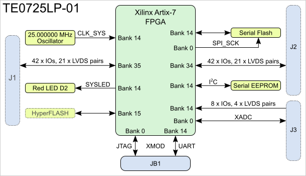
Figure 1: TE0725LP-01 Block Diagram.
...
Figure 2: TE0725LP-01 FPGA module (Variant TE0725LP-01-100-2D depicted).
- XMOD header, JB1
- 14-pin header placeholder for connector, J3
- Xilinx Artix-7 FPGA, U1
- 1.8V, 256 MBit (32 MByte) quad SPI serial flash memory, U7
- Red LED (SYSLED), D2
- Cypress S26KS512S 512 MBit (64 MByte) 1.8V HyperFlash™ memory, U4 (optional)
- Low-power programmable oscillator @25.000000 MHz, U3
- Low VIN high-efficiency step-down converter (1.5A max.), U5
- Low VIN high-efficiency step-down converter (1.5A max.), U6 (optional)
- 50-pin header placeholder for breadboard connector, J1
- 50-pin header placeholder for breadboard connector, J2
- Ultra-low supply-current voltage monitor with optional watchdog, U8
- 128KBit I2C CMOS serial EEPROM, U2
| Scroll Pagebreak |
|---|
Initial Delivery State
...
Table 1: Module initial delivery state of programmable on-board devices.
Boot Process
By default the configuration mode pins of the FPGA are set to Master SPI mode, hence the FPGA is configured from serial QSPI flash memory at system start-up. The JTAG interface of the module is provided for storing the initial FPGA configuration data to the QSPI flash memory.
Signals, Interfaces and Pins
I/Os on Pin Headers
I/O signals of the FPGA SoC's I/O banks connected to the board's pin headers:
| Bank | Type | Pin Header | I/O Signal Count | Bank Voltage |
|---|---|---|---|---|
| 14 | HR | J3 | 8 I/O's, 4 LVDS pairs | 1.8V |
| 34 | HR | J2 | 42 I/Os, 21 LVDS pairs | VCCIO34 |
| 35 | HR | J1 | 42 I/Os, 21 LVDS pairs | VCCIO35 |
Table 2: General overview of single ended and LVDS I/O signals connected to pin headers
PL I/O-Banks
| Bank | VCCIO | Used I/O's Count | Available On Connectors | Notes |
|---|---|---|---|---|
| 0 | 31.3V8V | 7 | 4 | 4 I/O's used for JTAG interface, 3 control signals (DONE, PROG_B, INIT). |
| 14 | 31.3V8V | 1222 | 11 | 8 I/O's (4 LVDS pairs) connected to J3, 3 I/O's to XMOD header JB1 (2 UART I/O's, 1 user I/O), 1 I/O to LED D2. |
| 15 | 1.8V | 18 | - | Used for optional HyperFlash™ U4. |
| 34 | User select | 42 | 42 | 0-Ohm resistor R17 option to select 1.8V I/O-bank VCCIO. |
| 35 | User select | 42 | 42 | 0-Ohm resistor R25 option to select 1.8V I/O-bank VCCIO. |
Table 3: General overview of PL I/O-bank signals.
JTAG Interface
JTAG access to the Xilinx Artix-7 device is provided through XMOD header JB1.
Header JB1 (2 x 6 pin) is compatible with XMOD-JTAG adapter TE0790. This adapter can be inserted from top onto the TE0725LP, if JB1 is fitted with male pin header. Optionally JB1 can be fitted with pin header from bottom, in that case the JTAG connector must be on the base board.
XMOD FTDI JTAG-Adapter Header JB1
The JTAG interface of the FPGA can be accessed via XMOD header JB1, so in use with the XMOD-FT2232H adapter-board TE0790 the FPGA can be configured via USB2.0 interface. The TE0790 board provides also an UART interface to the FPGA device which can be accessed by the USB2.0 interface of the adapter-board while the signals between these serial interfaces will be converted.
Following table describes the signals and interfaces of the XMOD header JB1:
| Pin Schematic Name | XMOD Header JB1 Pin | Note |
|---|---|---|
| F_TCK | C (pin J3-4) | - |
| F_TDO | D (pin J3-8) | - |
| F_TDI | F (pin J3-10) | - |
| F_TMS | H (pin J3-12) | - |
| UART_RXD | A (pin J3-3) | UART receive line, connected to PL I/O-bank 14. |
| UART_TXD | B (pin J3-7) | UART transmit line, connected to PL I/O-bank 14. |
| XMOD_E | E (pin J3-9) | User configurable, connected to PL I/O-bank 14, pin M17. |
| NRST | G (pin J3-11) | Assigned to 'PROG_B' (configuration-reset signal of FPGA) via IC U8. |
...
| Note |
|---|
Use Xilinx compatible TE0790 adapter board (designation TE-0790-xx with out 'L') to program the Xilinx Zynq devices. The TE0790 adapter board's CPLD have to be configured with the Standard variant of the firmware. Refer to the TE0790 Resources Site for further information and firmware download. |
UART Interface
UART interface is available on B2B connector JM2. With the TE0790 XMOD USB2.0 adapter, the UART signals can be converted to USB2.0 interface signals:
| UART Signal Schematic Name | B2B | XMOD Header JX1 | Pin Header J3 | Note |
|---|---|---|---|---|
| B14_L0 | JM2-99 | JX1-7 | J3-7 | UART-TX (transmit line) |
| B14_L25 | JM2-97 | JX1-3 | J3-3 | UART-RX (receive line) |
Table 6: UART interface signals.
QSPI Interface
The QSPI interface of the FPGA device is routed to and used by the on-module QSPI flash IC U7:
| SD IO Signal Schematic Name | FPGA I/O | Flash Memory (U7) Pin | Note |
|---|---|---|---|
| SPI-DQO | Bank 14, pin K17 | D3 | QSPI data |
| SPI-DQ1 | Bank 14, pin K18 | D2 | QSPI data |
| SPI-DQ2 | Bank 14, pin L14 | C4 | QSPI data |
| SPI-DQ3 | Bank 14, pin M14 | D4 | QSPI data |
| SPI_SCK | Bank 0, pin E9 | B2 | QSPI clock |
| SPI-CS | Bank 14, pin L13 | C2 | QSPI chip select |
...
Differential Analog Input
The TE0725LP FPGA module provides access to the XADC (Analog-to-Digital Converter) unit of the Xilinx FPGA via connector J3:
| I²C Signal Schematic Name | FPGA I/O | Connector J3 Pin | Notes |
|---|---|---|---|
| XADC_P | Bank 0, pin J10 (VP_0) | J3-14 | - |
| XADC_N | Bank 0, pin K9 (VN_0) | J3-13 | - |
...
On-board Peripherals
Quad SPI Flash Memory
On-module QSPI flash memory (U7) is provided by Micron Serial NOR Flash Memory N25Q256A with 256 MBit (32 MByte) storage capacity. This non volatile memory is used to store initial FPGA configuration. Besides FPGA configuration, remaining free flash memory can be used for user application and data storage. All four SPI data lines are connected to the FPGA allowing x1, x2 or x4 data bus widths. Maximum data rate depends on the selected bus width and clock frequency used.
HyperFlash™ Memory
On the TE0725LP FPGA module is optionally available a Cypress S26KS512S 512 MBit (64 MByte) 1.8V HyperFlash™ memory IC (U4). This flash memory IC is connected to the FPGA bank 15 via the Cypress specific HyperBus interface, which offers read bandwidth up to 333MByte/s.
EEPROM
A Microchip 24AA128 128 KBit (16 KByte) CMOS Serial EEPROM (U2). The device is organized as eight blocks of 16 KBit memory with a 2-wire serial interface connected on FPGA bank 14. The memory as is available for application use. It is accessible over I2C bus with slave device address 0x50.
System Clock Oscillator
A low-power SiTime programmable oscillator (U3) @25.000000 MHz configured on-module is connected to PL I/O-bank 14 and provides the system reference clock signal.
On-board LEDs
There is one red LED connected to the FPGA bank 14, pin M16. This LED is user configurable to indicate for example any system status.
| LED | Color | Signal Schematic Name | FPGA | Notes |
|---|---|---|---|---|
| D2 | Red | 'SYSLED' | Pin M16 | - |
Table 10: LEDs of the module.
Connectors
All connectors are are for 100mil headers, all connector locations are in 100mil (2.54mm) grid. The module's PCB provides footprints to mount and solder optional (B2B connector) headers, if those are not factory-fitted on module.
Power and Power-On Sequence
To power-up a module, power supply with minimum current capability of 1A is recommended.
Power Supply
TE0725LP needs one single power supply with nominal of 3.3V at the variant TE0725-01-100-2C or 1.8V at the variants TE0725LP-01-100-2D and TE0725LP-01-100-2D. Following diagram shows the dependencies of the power supply:
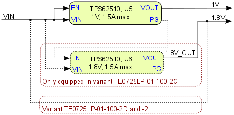
Figure 3: Module power supply dependencies
...
Table 11: Module power consumption
*TBD - To Be Determined.
Actual power consumption depends on the FPGA design and ambient temperature.
Power-On Sequence
There is no specific or special power-on sequence, single power source is needed as VIN.
Voltage Monitor Circuit
The 1.8V voltage level is monitored by the voltage monitor circuit U8, which generates the PROG_B signal to begin a new configuration sequence after reset of the FPGA. A manual reset is also possible by driving the connector pin JB1-11 ('NRST') to GND. Hence, by this pin a mounted XMOD adapter board can perform a reset on the FPGA module.
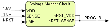
Figure 4: Voltage monitor circuit
...
Variants Currently In Production
| HTML |
|---|
<!--
Set correct link to the overview table of the product on english and german, if not available, set
https://shop.trenz-electronic.de/de/Produkte/Trenz-Electronic/
https://shop.trenz-electronic.de/en/Products/Trenz-Electronic/
--> |
| Trenz shop TE0xxx overview page | |
|---|---|
| English page | German page |
FPGA Chip Model
HyperFlash™ Memory (U4)
Table 12: Module variants production
...
Parameter | Min | Max | Units | Reference document |
|---|---|---|---|---|
VIN supply voltage (Variant TE0725LP-01-100-2C) | -0.3 | 4 | V | TI TPS62510 data sheet |
| VIN supply voltage (Variant TE0725LP-01-100-2D and -2L) | -0.3 | 2 | V | Xilinx datasheet DS181 / TI TPS62510 datasheet |
| HR I/O banks supply voltage (VCCO) | -0.5 | 3.6 | V | Xilinx datasheet DS181 |
| HR I/O banks input voltage (VCCIO single ended) | -0.4 | VCCO + 0.55 | V | Xilinx datasheet DS181 |
Storage Temperature | -40 | +100 | °C | LED SML-P11x series datasheet |
...
| Parameter | Min | Max | Units | Reference document |
|---|---|---|---|---|
| VIN supply voltage (Variant TE0725LP-01-100-2C) | 1.8 | 3.8 | V | TI TPS62510 data sheet |
| VIN supply voltage (Variant TE0725LP-01-100-2D and -2L) | 1.8 | 1.89 | V | Xilinx datasheet DS181 / TI TPS62510 datasheet |
| HR I/O banks supply voltage (VCCO) | 1.14 | 3.465 | V | Xilinx datasheet DS181 |
| HR I/O banks input voltage (VCCIO single ended) | -0.20 | VCCO + 0.20 | V | Xilinx datasheet DS181 |
| Operating Temperature | 0 | +85 | °C | Xilinx datasheet DS181 |
Table 14: Recommended operating conditions
...
Table 15: Module hardware revision history
Hardware revision number is printed on the PCB board together with the module model number separated by the dash.
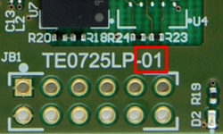
Figure 6: Module hardware revision number
...
Overview
Content Tools