Page History
...
Power supply with minimum current capability of 3A 4A for system startup is recommended.
...
Table 17: Power consumption
* TBD - To Be Determined soon with reference design setup.
Single 3.3V power supply with minimum current capability of 4A for system startup is recommended.
For the lowest power consumption and highest efficiency of the on-board DC-DC regulators it is recommended to power the module from one single 3.3V supply. All input power supplies should have a nominal value of 3.3V. Although the input power supplies can be powered up in any order, it is recommended to power them up simultaneously.
| Warning |
|---|
| To avoid any damage to the module, check for stabilized on-board voltages should be carried out (i.e. power good and enable signals) before powering up any Zynq's I/O bank voltages VCCO_x. All I/Os should be tri-stated during power-on sequence. |
Power Distribution Dependencies
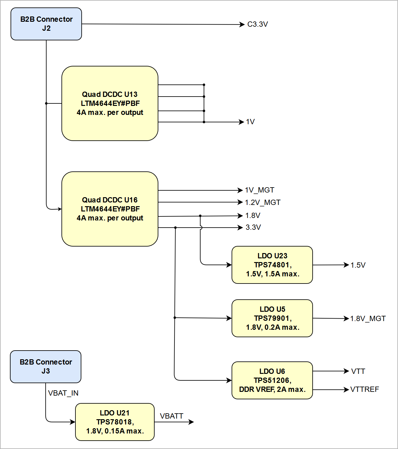
The Trenz TE0782 SoM is equipped with two quad DC-DC voltage regulators to generate required on-board voltage levels 1V, 3.3V, 1.8V, 1.2V_MGT, 1V_MGT. Additional voltage regulators are used to generate voltages 1.5V, VTT, VTTREF and 1.8V_MGT.
The power supply voltage 'C3.3V' of System Controller CPLD of the SoM have to be externally supplied with 3.3V nominal.
There are following dependencies how the initial voltages of the power rails on the B2B connectors are distributed to the on-board DC-DC converters, which power up further DC-DC converters and the particular on-board voltages:
| Scroll Titlescroll-title | ||||||||||||||||||||||||||||||||
|---|---|---|---|---|---|---|---|---|---|---|---|---|---|---|---|---|---|---|---|---|---|---|---|---|---|---|---|---|---|---|---|---|
| ||||||||||||||||||||||||||||||||
|
See also Xilinx datasheet DS191 for additional information. User should also check related base board documentation when intending base board design for TE0782 module.
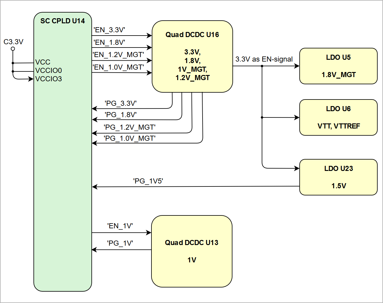
Power-On Sequence
The TE0820 SoM meets the recommended criteria to power up the Xilinx Zynq chip properly by keeping a specific sequence of enabling the on-board DC-DC converters dedicated to the particular functional units of the Zynq chip and powering up the on-board voltages.
base board documentation when intending base board design for TE0782 module.
Power-On Sequence
Power-on sequence is handled by the System Controller CPLD using "Power good"-signals from the voltage regulatorsFollowing diagram clarifies the sequence of enabling the particular on-board voltages, which will power-up in descending order as listed in the blocks of the diagram:
| Scroll Title | ||||||||||||||||||||||||||||||||||
|---|---|---|---|---|---|---|---|---|---|---|---|---|---|---|---|---|---|---|---|---|---|---|---|---|---|---|---|---|---|---|---|---|---|---|
| ||||||||||||||||||||||||||||||||||
|
...
It is important that all carrier board I/Os are 3-stated at power-on until System Controller CPLD sets PGOOD signal high (B2B connector JM1, pin 30), or 3.3V is present on B2B connector JM2 pins 10 and 12, indicating that all on-module voltages have become stable and module is properly powered up.
...
|
Power Rails
| Power Rail Name on B2B Connector | J1 Pins | J2 Pins | J3 Pins | Direction | Notes |
|---|---|---|---|---|---|
| VIN | - | 165, 166, 167, 168 | - | Input | external power supply voltage |
| C3.3V | - | 147, 148 | - | Input | external 3.3V power supply voltage |
| 3.3V | - | 111, 112, 123, 124, 135 136 169, 170, 171, 172 | - | Output | internal 3.3V voltage level |
| 1.8V | 169, 170, 171, 172 | - | - | Output | internal 1.8V voltage level |
| VCCIO_10 | - | - | 99, 100 | Input | high range I/O bank voltage |
| VCCIO_11 | - | - | 159, 160 | Input | high range I/O bank voltage |
| VCCIO_12 | - | 159, 160 | - | Input | high range I/O bank voltage |
| VCCIO_13 | - | 99, 100 | - | Input | high range I/O bank voltage |
| VCCIO_33 | 99, 100 | - | - | Input | high performance I/O bank voltage |
| VCCIO_34 | 159, 160 | - | - | Input | high performance I/O bank voltage |
| VBAT_IN | - | - | 124 | Input | backup battery voltage |
...
Overview
Content Tools