Page History
...
- Xilinx Kintex-7 XC7K160T, XC7K325T or XC7K410T FPGA SoC
- Large number of configurable I/Os are provided via rugged HPC FMC connector
- Dual ARM Cortex-A9 MPCore
- 1 GByte RAM (32-Bit wide DDR3)
- 32 MByte QSPI Flash memory
- 2 x Hi-Speed USB2 ULPI transceiver PHY
- 2 x Gigabit (10/100/1000 Mbps) Ethernet transceiver PHY
- 4 GByte eMMC (optional up to 64 GByte)
- 2 x MAC-address EEPROMs
- Optional 2x 64 MByte HyperFLASH or 2x 8 MByte HyperRAM (max 2x 32 MByte HyperRAM)
- Temperature compensated RTC (real-time clock)
- Si5338A programmable quad PLL clock generator for GTX transceiver clocks
- Plug-on module with 3 x 160-pin high-speed strips
- 16 GTX high-performance transceiver
- 2x GT transceiver clock inputs
- 254 FPGA I/O's (125 LVDS pairs)
- 16 GTX high-performance transceiver
- 2x MGT transceiver clock inputs
- 254 FPGA HR I/O's (125 LVDS pairs)
- Si5338A programmable quad PLL clock generator for GTX transceiver clocks
- On-board high-efficiency switch-mode DC-DC On-board high-efficiency switch-mode DC-DC converters
- System management
- eFUSE bit-stream encryption
- AES bit-stream encryption
- Evenly-spread supply pins for good signal integrity
- User LED
- PCI Express 2.0 x8 card with maximum throughput of 4 GB/s
- FMC High Pin Count (HPC) connector
- 8 FPGA MGT lanes available on PCIe interface
- DDR3 SO-DIMM SDRAM socket
- 256-Mbit (32-MByte) Quad SPI Flash memory (for configuration and operation) accessible through:
- FPGA
- JTAG port (SPI indirect, bus width x4)
- External clock input via SMA coaxial connector
- 28 GTH transceivers, each with up to 13.1 Gbit/s data transmission rate
- FPGA configuration through:
- JTAG connector
- Quad SPI Flash memory
- Programmable quad clock generator
TI LMK04828B ultra low-noise JESD204B compliant clock jitter cleaner
- On-board high-efficiency DC-DC converters
- Up to 202 FPGA I/O pins available on FMC connector (up to 101 LVDS pairs possible)
- System management and power sequencing
- AES bit-stream encryption
- eFUSE bit-stream encryption
- Xilinx Kintex UltraScale FPGA (XCKU035 or XCKU040)
- 2 banks of 1024 MByte DDR4 SDRAM, 32bit wide memory interface
- 512 Mbit (64 MByte) QSPI Flash
- 3 x Samtec Razor Beam LSHM B2B, 260 terminals total
- 60 x HR I/Os
- 84 x HP I/Os
- 8 x GTH transceiver lanes (TX/RX)
- 2 x MGT external clock inputs - Clocking
- Si5338 - 4 output PLLs, GT and PL clocks
- 200 MHz LVDS oscillator - All power supplies on-board, single power source operation
- Evenly spread supply pins for optimized signal integrity
- Size: 40 x 50 mm
- 3 mm mounting holes for skyline heat spreader
- Rugged for industrial applications
...
| Scroll Title | ||||||||||||||||||||||||||||||||
|---|---|---|---|---|---|---|---|---|---|---|---|---|---|---|---|---|---|---|---|---|---|---|---|---|---|---|---|---|---|---|---|---|
| ||||||||||||||||||||||||||||||||
|
...
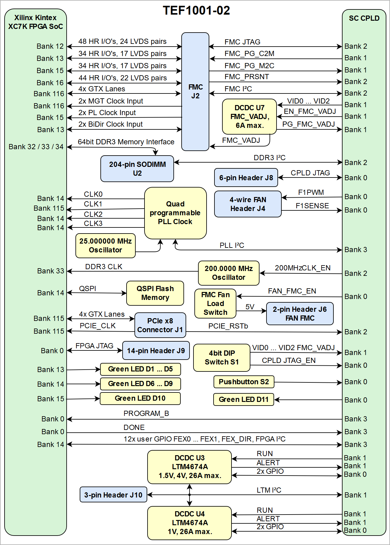
I/O signals connected to the SoCs I/O bank and B2B FMC connector J2:
| FPGA Bank | Type | I/O Signal Count | Bank VCCO Voltage | Notes | ||||||
|---|---|---|---|---|---|---|---|---|---|---|
| 6412 | HR | 48 IO's, 24 LVDS pairs | B64FMC_VCCOVADJ | Supplied by the carrier board | Bank voltage supplied by DC-DC converter U7 | |||||
| 1365 | HR | 8 34 IO's | 3.3V | On-module power supply | ||||||
| 65 | HR | 4 IO's | 3.3V | On-module power supply | ||||||
| , 17 LVDS pairs | FMC_VADJ | |||||||||
| 15 | HR | 34 | 66 | HP | 16 IO's, 8 17 LVDS pairs | B66FMC_VCCO | Supplied by the carrier board | 67 | HP | VADJ |
| 16 | HR | 44 48 IO's, 24 22 LVDS pairs | B67VIO_B_VCCOFMC | Supplied by the carrier board | ||||||
| 67 | HP | 2 IO's | B67_VCCO | Supplied by the carrier board | ||||||
| 68 | HP | 18 IO's, 9 LVDS pairs | B68_VCCO | Supplied by the carrier boardBank voltage supplied by FMC connector J2 |
Table 2: General overview of FPGA's PL I/O signals connected to the FMC connector
...
MGT (Multi Gigabit Transceiver) lane consists of one transmit and one receive (TX/RX) differential pairs, two signals each or four signals total per one MGT lane. The MGT lanes are connected to the FMC connector and to the PCIe x8 connector. Following table lists lane number, MGT bank number, transceiver type, signal schematic name, connector and FPGA pins connection:
| Lane | Bank | Type | Signal Name | PCIe Connector Pin | FPGA Pin | ||
|---|---|---|---|---|---|---|---|
| 0 | 115 | GTX |
|
|
| ||
| 1 | 115 | GTX |
|
|
| ||
| 2 | 115 | GTX |
|
|
| ||
| 3 | 115 | GTX |
|
|
| ||
| Lane | 116Bank | Type | Signal Name | FMC Connector Pin | FPGA Pin | ||
| 0 | 116 | GTX |
| GTX |
|
|
|
| 51 | 116 | GTX |
|
|
| ||
| 62 | 116 | GTX |
|
|
| ||
| 73 | 116 | GTX |
|
|
|
Table 3: FPGA to B2B connectors routed MGT lanes overview
Below are listed MGT banks reference clock sources:
| Clock signal | Bank | Source |
|---|
| FPGA Pin |
|---|
| Notes |
|---|
| MGTCLK_5338 |
| _P |
- MGTHRXP0_117, N4
- MGTHRXN0_117, N3
- MGTHTXP0_117, M2
- MGTHTXN0_117, M1
- J2A-C6
- J2A-C7
- J2A-C2
- J2A-C3
- DP1_M2C_P
- DP1_M2C_N
- DP1_C2M_P
- DP1_C2M_N
- MGTHRXP1_117, L4
- MGTHRXN1_117, L3
- MGTHTXP1_117, K2
- MGTHTXN1_117, K1
- J2A-A2
- J2A-A3
- J2A-A22
- J2A-A23
- DP2_M2C_P
- DP2_M2C_N
- DP2_C2M_P
- DP2_C2M_N
- MGTHRXP2_117, K6
- MGTHRXN2_117, K5
- MGTHTXP2_117, H2
- MGTHTXN2_117, H1
- J2A-A6
- J2A-A7
- J2A-A26
- J2A-A27
- DP3_M2C_P
- DP3_M2C_N
- DP3_C2M_P
- DP3_C2M_N
- MGTHRXP3_117, J4
- MGTHRXN3_117, J3
- MGTHTXP3_117, F2
- MGTHTXN3_117, F1
- J2A-A10
- J2A-A11
- J2A-A30
- J2A-A31
- DP4_M2C_P
- DP4_M2C_N
- DP4_C2M_P
- DP4_C2M_N
- MGTHRXP0_118, G4
- MGTHRXN0_118, G3
- MGTHTXP0_118, D2
- MGTHTXN0_118, D1
- J2A-A14
- J2A-A15
- J2A-A34
- J2A-A35
| Lane | FPGA Bank | Type | Signal Name | FPGA Pin | FMC Pin |
|---|---|---|---|---|---|
| 5 | 118 | GTH |
|
|
|
| 6 | 118 | GTH |
|
|
|
| 7 | 118 | GTH |
|
|
|
| 8 | 116 | GTH |
|
|
|
| 9 | 116 | GTH |
|
|
|
...
- PER0_P
- PER0_N
- PET0_P
- PET0_N
...
- MGTHRXP3_115, AB2
- MGTHRXN3_115, AB1
- MGTHTXP3_115, AC4
- MGTHTXN3_115, AC3
...
- J1-A16
- J1-A17
- J1-B14
- J1-B15
...
- PER1_P
- PER1_N
- PET1_P
- PET1_N
...
- MGTHRXP2_115, AD2
- MGTHRXN2_115, AD1
- MGTHTXP2_115, AE4
- MGTHTXN2_115, AE3
...
- J1-A21
- J1-A22
- J1-B19
- J1-B20
...
- PER2_P
- PER2_N
- PET2_P
- PET2_N
...
- MGTHRXP1_115, AF2
- MGTHRXN1_115, AF1
- MGTHTXP1_115, AF6
- MGTHTXN1_115, AF5
...
- J1-A25
- J1-A26
- J1-B23
- J1-B24
...
- PER3_P
- PER3_N
- PET3_P
- PET3_N
...
- MGTHRXP0_115, AH2
- MGTHRXN0_115, AH1
- MGTHTXP0_115, AG4
- MGTHTXN0_115, AG3
...
- J1-A29
- J1-A30
- J1-B27
- J1-B28
...
- PER4_P
- PER4_N
- PET4_P
- PET4_N
...
- MGTHRXP3_114, AK2
- MGTHRXN3_114, AK1
- MGTHTXP3_114, AJ4
- MGTHTXN3_114, AJ3
...
- J1-A35
- J1-A36
- J1-B33
- J1-B34
...
- PER5_P
- PER5_N
- PET5_P
- PET5_N
...
- MGTHRXP2_114, AM2
- MGTHRXN2_114, AM1
- MGTHTXP2_114, AL4
- MGTHTXN2_114, AL3
...
- J1-A39
- J1-A40
- J1-B37
- J1-B38
...
- PER6_P
- PER6_N
- PET6_P
- PET6_N
...
- MGTHRXP1_114, AN4
- MGTHRXN1_114, AN3
- MGTHTXP1_114, AM6
- MGTHTXN1_114, AM5
...
- J1-A43
- J1-A44
- J1-B41
- J1-B42
...
- PER7_P
- PER7_N
- PET7_P
- PET7_N
...
- MGTHRXP0_114, AP2
- MGTHRXN0_114, AP1
- MGTHTXP0_114, AP6
- MGTHTXN0_114, AP5
...
- J1-A47
- J1-A48
- J1-B45
- J1-B46
Below are listed MGT banks reference clock sources:
...
Table 4: MGT reference clock sources
| Clock Signal | MGT Bank | Source | FPGA Pin | Notes |
|---|---|---|---|---|
| MGTCLK_5338_P | 115 | U13, CLK1A | MGTREFCLK0P_115, AB6 | On-board Si5338A. |
| MGTCLK_5338_N | 115 | U13, CLK1B | MGTREFCLK0N_115, AB5 | On-board Si5338A. |
| PCIE_CLK_P | 115 | J1-A13, REFCLK+ | MGTREFCLK1P_115, AD6 | External clock from PCIe slot. |
| PCIE_CLK_N | 115 | J1-A14, REFCLK- | MGTREFCLK1N_115, AD6 | External clock from PCIe slot. |
| CLK_SYNTH_DCLKOUT4_P | 116 | U9, DCLKout4 | MGTREFCLK0P_116, T6 | On-board LMK04828B. |
| CLK_SYNTH_DCLKOUT4_N | 116 | U9, DCLKout4* | MGTREFCLK0N_116, T6 | On-board LMK04828B. |
| GBTCLK0_M2C_P | 117 | J2-D4 | MGTREFCLK0P_117, M6 | External clock from FMC connector. |
| GBTCLK0_M2C_N | 117 | J2-D5 | MGTREFCLK0N_117, M5 | External clock from FMC connector. |
| GBTCLK1_M2C_P | 117 | J2-B20 | MGTREFCLK1P_117, P6 | External clock from FMC connector. |
| GBTCLK1_M2C_N | 117 | J2-B21 | MGTREFCLK1N_117, P5 | External clock from FMC connector. |
| CLK_SYNTH_SDCLKOUT7_P | 118 | U9, DCLKout7 | MGTREFCLK0P_118,F6 | On-board LMK04828B. |
| CLK_SYNTH_SDCLKOUT7_N | 118 | U9, DCLKout7* | MGTREFCLK0N_118,F5 | On-board LMK04828B. |
| MGTCLK2_5338_P | 118 | U13, CLK3A | MGTREFCLK1P_118, H6 | On-board Si5338A. |
| MGTCLK2_5338_N | 118 | U13, CLK3B | MGTREFCLK1N_118, H5 | On-board Si5338A. |
JTAG Interface
There are three JTAG interfaces available on the TEF1001 board:
...
CPLD JTAG
VCCIO: 3.3V
Connector: J8
...
J8-4
...
FPGA JTAG
VCCIO: 1.8V
Connector: J9
...
FMC JTAG
VCCIO: 3.3V
Connector: J2
...
| 115 | U13, CLK1A | MGTREFCLK0P_115, H6 | Supplied by on-board Si5338A | |
| MGTCLK_5338_N | U13, CLK1B | MGTREFCLK0N_115, H5 | ||
| PCIE_CLK_P | 115 | J1-A13, REFCLK+ | MGTREFCLK1P_115, K6 | External clock from PCIe slot |
| PCIE_CLK_N | J1-A14, REFCLK- | MGTREFCLK1N_115, K6 | ||
| GBTCLK0_M2C_P | 116 | J2-D4 | MGTREFCLK0P_116, D6 | External clock from FMC connector |
| GBTCLK0_M2C_N | J2-D5 | MGTREFCLK0N_116, D5 | ||
| GBTCLK1_M2C_P | 116 | J2-B20 | MGTREFCLK1P_116, F6 | External clock from FMC connector |
| GBTCLK1_M2C_N | J2-B21 | MGTREFCLK1N_116, F5 |
Table 4: MGT reference clock sources
JTAG Interface
There are three JTAG interfaces available on the TEF1001 board:
| JTAG Interface | Signal Schematic Name | JTAG Connector Pin | Connected to |
|---|---|---|---|
CPLD JTAG VCCIO: 3.3V Connector: J8 | CPLD_JTAG_TMS | J8-1 | SC CPLD, bank 0, pin 90 |
| CPLD_JTAG_TDI | J8-2 | SC CPLD, bank 0, pin 94 | |
| CPLD_JTAG_TDO | J8-3 | SC CPLD, bank 0, pin 95 | |
| CPLD_JTAG_TCK | J8-4 | SC CPLD, bank 0, pin 91 | |
FPGA JTAG VCCIO: 1.8V Connector: J9 | FPGA_JTAG_TMS | J9-4 | FPGA, bank 0, pin N9 |
| FPGA_JTAG_TCK | J9-6 | FPGA, bank 0, pin M8 | |
| FPGA_JTAG_TDO | J9-8 | FPGA, bank 0, pin N8 | |
| FPGA_JTAG_TDI | J9-10 | FPGA, bank 0, pin L8 | |
FMC JTAG VCCIO: 3.3V Connector: J2 | FMC_TRST | J2-D34 | SC CPLD, bank 2, pin 36 |
| FMC_TCK | J2-D29 | SC CPLD, bank 2, pin 27 | |
| FMC_TMS | J2-D33 | SC CPLD, bank 2, pin 28 | |
| FMC_TDI | J2-D30 | SC CPLD, bank 2, pin 31 | |
| FMC_TDO | J2-D31 | SC CPLD, bank 2, pin 32 |
Table 5: JTAG interface signals
System Controller CPLD I/O Pins
Special purpose pins are connected to the System Controller CPLD and have following default configuration:
| Pin Name | SC CPLD Direction | Function | Default Configuration |
|---|---|---|---|
| JTAG_EN | Input | JTAG select | Low for normal operation |
| nRST_SC0 | Input | Reset | Low active board reset input |
| SC1 | - | - | not currently used ('BOOTMODE' in default B2B pin out') |
| SC2 | Input / Output | - | Power good signal ('PGOOD' in default B2B pin out) |
| SC3 | Input | - | Power enable pin ('EN1' in default B2B pin out) |
| SC4 | - | - | not currently used ('NOSEQ' in default B2B pin out') |
| F_TCK | Output | JTAG signals between | B2B JTAG signals are forwarded to the FPGA through SC CPLD. |
| F_TMS | Output | ||
| F_TDI | Output | ||
| F_TDO | Input | ||
| TCK | Input | JTAG signals between SC CPLD and B2B connector | Program FPGA or SC CPLD depending on pin JTAGMODE. |
| TMS | Input | ||
| TDI | Input | ||
| TDO | Output | ||
| PROG_B | Output | FPGA configuration | PL configuration reset signal. |
| DONE | Input | FPGA configuration done | PL configuration completed. |
| PUDC_B | Output | Pull up during configuration | PL I/O's are 3-stated until configuration of the FPGA completes. |
| INIT_B | Input | Initialization done | Low active FPGA initialization pin or configuration error signal. |
| EN_PL | Input | Enable PL Power DC-DC converters | Set to contant logical high. |
| CPLD_IO | Output | user I/O | Connected to FPGA Bank 45, pin P28. |
Table 6: System Controller CPLD I/O pins
| CPLD Functionality | Interface | Designated CPLD Pins | Connected to | Notes |
|---|---|---|---|---|
| I2C interface between on-board peripherals and FPGA | I2C |
|
| VCCIO: 1V8, all with pull-up to 1V8. Following devices and connectors are linked to the FPGA_IIC I2C interface:
Note: FPGA_IIC_OE must kept high for I2C operation. For I2C slave device addresses refer to the component datasheets. |
User I/Os External LVDS pairs | 10 I/Os 5 x LVDS pairs |
|
| Can also be used for single-ended signaling. |
User I/Os Internal LVDS pairs | 13 I/Os 6 x LVDS pairs |
|
| VCCIO: 1V8 Can also be used for single-ended signaling. FPGA bank 18 has also reference clock input from FMC connector (CLK2, CLK3) and clock synthesizer U9 (FCLK). Internal signal assignment: FEX_DIR <= FMC_PRSNT_M2C_L |
| FPGA programming control and state | 2 I/Os |
|
| VCCIO: 1V8 |
| I2C interface to programmable quad clock generator | I2C |
|
| VCCIO: 1V8 Only PLL_SDA has 1V8 pull-up. |
| Fan PWM control J4 | 2 I/Os |
|
| Internal signal assignment:
|
| Button S2 | 1 I/O |
|
| Functionality depends on CPLD firmware, activating pin PROGRAM_B (active low) and LED1 in standard configuration. |
| LED1 | 1 I/O |
|
| Fast blinking, when FPGA is not programmed. Internal signal assignment:
|
PCIe control line RESET_B | 1 I/O |
|
| Internal signal assignment:
|
Control interface to clock synthesizer U9 (TI LMK04828B) | SPI (3 I/Os), 4 I/Os |
|
| Pull up to 3V3PCI.
|
| Control Interface to DC-DC converters U3 and U4 (both LTM4676) | I2C (2 I/Os), 2 I/Os |
|
| 3V3 pull-ups. LTM I2C interface is also accessible trough header J10. LTM1_ALERT and LTM2_ALERT signals are not used. |
| Power-on sequence and monitoring | 6 I/Os |
|
| Sequence of the supply voltages depend on the System Controller CPLD firmware. EN_1V8, EN_3V3 and EN_FMC_VADJ will be set simultaneously at start-up. PG signals will not be evaluated. |
Table 5: JTAG interface signals
System Controller CPLD I/O Pins
Special purpose pins are connected to the System Controller CPLD and have following default configuration:
...
JTAG signals between
SC CPLD and FPGA
...
Program FPGA or SC CPLD depending on pin JTAGMODE.
...
PL I/O's are 3-stated until configuration of the FPGA completes.
...
Low active FPGA initialization pin or configuration error signal.
...
For detailed function of the pins and signals, the internal signal assignment and the implemented logic, look to the Wiki reference page of the module's SC CPLD or into its bitstream file.
...
See also the current available variants on the Trenz Electronic shop page
| Trenz shop TE0841 TEF1001 overview page | |
|---|---|
| English page | German page |
...
Overview
Content Tools