...
Intel® MAX 10 Commercial [10M08SAU169C8G]
SDRAM Memory up to 64Mb, 166MHz
Dual High Speed USB to Multipurpose UART/FIFO IC
64Mb Quad SPI Flash
4Kb EEPROM Memory
8x User LED
Micro USB2 Receptacle 90
16 Bit 500kSPS 500 kSPS Analog to Digital Converter
2x SMA Female Connector
I/O interface:
Power Supply:
- Dimension: 25m x 86.5m
Others:
...
| Scroll Title |
|---|
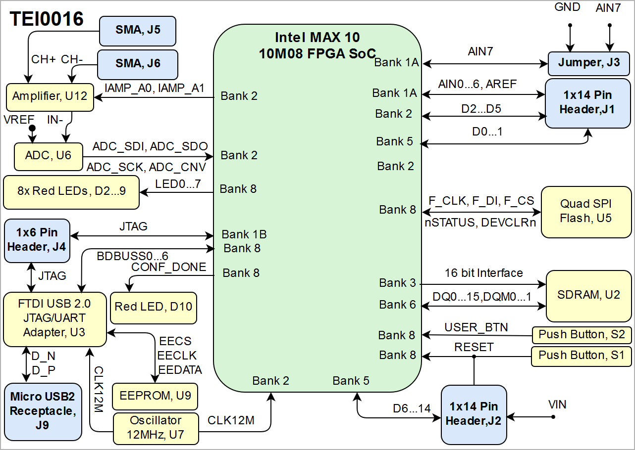
| anchor | Figure_OV_BD |
|---|
| title | TEI0016 block diagram |
|---|
|
| Scroll Ignore |
|---|
| draw.io Diagram |
|---|
| border | false |
|---|
| viewerToolbar | true |
|---|
| |
|---|
| fitWindow | false |
|---|
| diagramDisplayName | |
|---|
| lbox | true |
|---|
| revision | 68 |
|---|
| diagramName | TEI0016_OV_BD |
|---|
| simpleViewer | false |
|---|
| width | |
|---|
| links | auto |
|---|
| tbstyle | hidden |
|---|
| diagramWidth | 641 |
|---|
|
|
| Scroll Only |
|---|
|
|
...
The FPGA configuration for Intel MAX 10 FPGAs can be stored through JTAG interface either in external configuration device (active serial configuration memory SPI Flash U5) or on the FPGA itself since the Intel MAX 10 FPGA offers non-volatile memory on chip. The FPGA configuration is loaded from the non-volatile memory when the board is powered up.
...
| Scroll Title |
|---|
| anchor | Table_OBP_IOs |
|---|
| title | FPGA I/O Banks |
|---|
|
| Scroll Table Layout |
|---|
| orientation | portrait |
|---|
| sortDirection | ASC |
|---|
| repeatTableHeaders | default |
|---|
| style | |
|---|
| widths | |
|---|
| sortByColumn | 1 |
|---|
| sortEnabled | false |
|---|
| cellHighlighting | true |
|---|
|
| FPGA Bank | I/O Signal Count | Connected to | Notes |
|---|
| Bank 1A | 7 | 1x14 Pin header, J1 | AIN0...6 | | 1 | Jumper, J3 | AIN7 | | Bank 1B | 5 | 1x6 Pin header, J4 | JTAG_EN, TDI, TDO, TMS, TCK | Bank 2
| 4 | 1x14 Pin header, J1 | D2...5 | | 5 | A2DADC, U15 | ADC_EN, ADC_SDI, ADC_SDO, ADC_SCK, ADC_CNV | | 1 | 12MHz Oscillator, U7 | CLK12M | | 2 | Amplifier, U12 | nIAMP_A0, nIAMP_A1 | | Bank 3 | 22 | SDRAM, U2 | RAM_ADDR_CMD | | Bank 5 | 9 | 1x14 Pin header, J2 | DIO6...14 | | 2 | 1x14 Pin header, J1 | DIO0...1 | | 1 | D12_R | DIO12 | | Bank 6 | 16 | SDRAM, U2 | DQ0...15 | | 2 | SDRAM, U2 | DQM0...1 | | 1 | D11_R | DIO11 | Bank 8
| 8 | User Red LEDs, D2...9 | LED0...7 | | 6 | SPI Flash, U5 | F_CS, F_CKCLK, F_DI, F_DO, nSTATUS, DEVCLRn | | 1 | Red LED, D10 | CONF_DONE | | 6 | FTDI JTAG/UART Adapter, U3 | BDBUS0...5 | | 1 | Push Button, S2 | USER_BTN |
|
...
| Scroll Title |
|---|
| anchor | Table_OBP |
|---|
| title | On board peripherals |
|---|
|
| Scroll Table Layout |
|---|
| orientation | portrait |
|---|
| sortDirection | ASC |
|---|
| repeatTableHeaders | default |
|---|
| style | |
|---|
| widths | |
|---|
| sortByColumn | 1 |
|---|
| sortEnabled | false |
|---|
| cellHighlighting | true |
|---|
|
|
...
| Scroll Title |
|---|
| anchor | Table_OBP_FTDI |
|---|
| title | FTDI chip interfaces and pins |
|---|
|
| Scroll Table Layout |
|---|
| orientation | portrait |
|---|
| sortDirection | ASC |
|---|
| repeatTableHeaders | default |
|---|
| style | |
|---|
| widths | |
|---|
| sortByColumn | 1 |
|---|
| sortEnabled | false |
|---|
| cellHighlighting | true |
|---|
|
| FTDI Chip U3 Pin | Signal Schematic Name | Connected to | Notes |
|---|
| ADBUS0 | TCK | FPGA bank 1B, pin G2 | JTAG interface | | ADBUS1 | TDI | FPGA bank 1B, pin F5 | | ADBUS2 | TDO | FPGA bank 1B, pin F6 | | ADBUS3 | TMS | FPGA bank 1B, pin G1 | | BDBUS0 | BDBUS0 | FPGA bank 8, pin A4 | user configurable | | BDBUS1 | BDBUS1 | FPGA bank 8, pin B4 | user configurable | | BDBUS2 | BDBUS2 | FPGA bank 8, pin B5 | user configurable | | BDBUS3 | BDBUS3 | FPGA bank 8, pin A6 | user configurable | | BDBUS4 | BDBUS4 | FPGA bank 8, pin B6 | user configurable | | BDBUS5 | BDBUS5 | FPGA bank 8, pin A7 | user configurable |
|
...
SPI Flash
On-board serial configuration memory (U5) is provided by Winbond with 64 MBit (8 MByte) storage capacity. This non volatile memory is used to store initial FPGA configuration via JTAG interface. The memory is connected to FPGA bank 8 via SPI interface.
...
| Scroll Title |
|---|
| anchor | Table_OBP_A2DADC |
|---|
| title | A2D ADC converter interface and pins |
|---|
|
| Scroll Table Layout |
|---|
| orientation | portrait |
|---|
| sortDirection | ASC |
|---|
| repeatTableHeaders | default |
|---|
| style | |
|---|
| widths | |
|---|
| sortByColumn | 1 |
|---|
| sortEnabled | false |
|---|
| cellHighlighting | true |
|---|
|
| Pins | Connected to | Notes |
|---|
IN+ | U8, VOUT | VREF_ADC | | IN- | U12, VOUT |
| | SDI | Bank 2, ADC_SDI |
| | SDO | Bank 2, ADC_SDO |
| | SCK | Bank 2, ADC_SCK |
| | CNV | Bank 2, ADC_CNV |
|
|
...
| Scroll Title |
|---|
| anchor | Figure_PWR_PD |
|---|
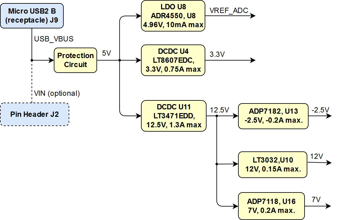
| title | Power Distribution |
|---|
|
| Scroll Ignore |
|---|
| draw.io Diagram |
|---|
| border | false |
|---|
| viewerToolbar | true |
|---|
| |
|---|
| fitWindow | false |
|---|
| diagramDisplayName | |
|---|
| lbox | true |
|---|
| revision | 23 |
|---|
| diagramName | TEI0016_PWR_PD |
|---|
| simpleViewer | false |
|---|
| width | |
|---|
| links | auto |
|---|
| tbstyle | hidden |
|---|
| diagramWidth | 640 |
|---|
|
|
| Scroll Only |
|---|
|
|
...
| Scroll Title |
|---|
| anchor | Table_PWR_BV |
|---|
| title | Zynq Intel Max 10 SoC bank voltages. |
|---|
|
| Scroll Table Layout |
|---|
| orientation | portrait |
|---|
| sortDirection | ASC |
|---|
| repeatTableHeaders | default |
|---|
| style | |
|---|
| widths | |
|---|
| sortByColumn | 1 |
|---|
| sortEnabled | false |
|---|
| cellHighlighting | true |
|---|
|
| Schematic Name | | Notes |
|---|
| Bank 1A | VCCIO1A | 3.3V |
| | Bank 1B | VCCIO1B | 3.3V |
| | Bank 2 | VCCIO2 | 3.3V |
| | Bank 3 | VCCIO3 | 3.3V |
| | Bank 5 | VCCIO5 | 3.3V |
| | Bank 6 | VCCIO6 | 3.3V |
| | Bank 8 | VCCIO8 | 3.3V |
|
|
...
| Scroll Title |
|---|
| anchor | Table_TS_AMR |
|---|
| title | Absolute maximum ratings |
|---|
|
| Scroll Table Layout |
|---|
| orientation | portrait |
|---|
| sortDirection | ASC |
|---|
| repeatTableHeaders | default |
|---|
| style | |
|---|
| widths | |
|---|
| sortByColumn | 1 |
|---|
| sortEnabled | false |
|---|
| cellHighlighting | true |
|---|
|
| Symbols | Description | Min | Max | Unit | Reference Document |
|---|
VIN | Supply voltage | 4.75 | 5.25 | V |
| | VCC_ONE | Supply voltage for core and periphery through on-die voltage
regulator | -0.5 | 3.9 | V | Intel MAX 10 datasheet | | VCCIO | Supply voltage for input and output buffers | -0.5 | 3.9 | V | Intel MAX 10 datasheet | | VCCA | Supply voltage for phase-locked loop (PLL) regulator and ADC | -0.5 | 3.9 | V | Intel MAX 10 datasheet | | V_AN_IN | Analog Input Voltage on ADC IC U15 U6 pins | -0.1 | 5.1 | V | ADAQ7988B datasheet | | V_REF | Analog reference voltage on IC U15U6 | -3.2 | 7.7 | V | ADAQ7988B datasheet | | CH1+ | Analog input voltage on amplifier U12 pin 10 |
| 25 | V | AD8251ARMZ datasheet | | CH1- | Analog input voltage on amplifier U12 pin 10 |
| 25 | V | AD8251ARMZ datasheet | T_STG | Storage Temperature | -40 | +85 | °C |
|
|
Recommended Operating Conditions
...