...
Intel® MAX 10 Commercial [10M08SAU169C8G]
SDRAM Memory up to 64Mb, 166MHz
Dual High Speed USB to Multipurpose UART/FIFO IC
64Mb Quad SPI Flash
4Kb EEPROM Memory
8x User LED
Micro USB2 Receptacle 90
16 Bit 500 kSPS Analog to Digital Converter
2x SMA Female Connector
I/O interface: 23x GPIO
Power Supply:
- Dimension: 25m x 86.5m
Others:
...
| Scroll Title |
|---|
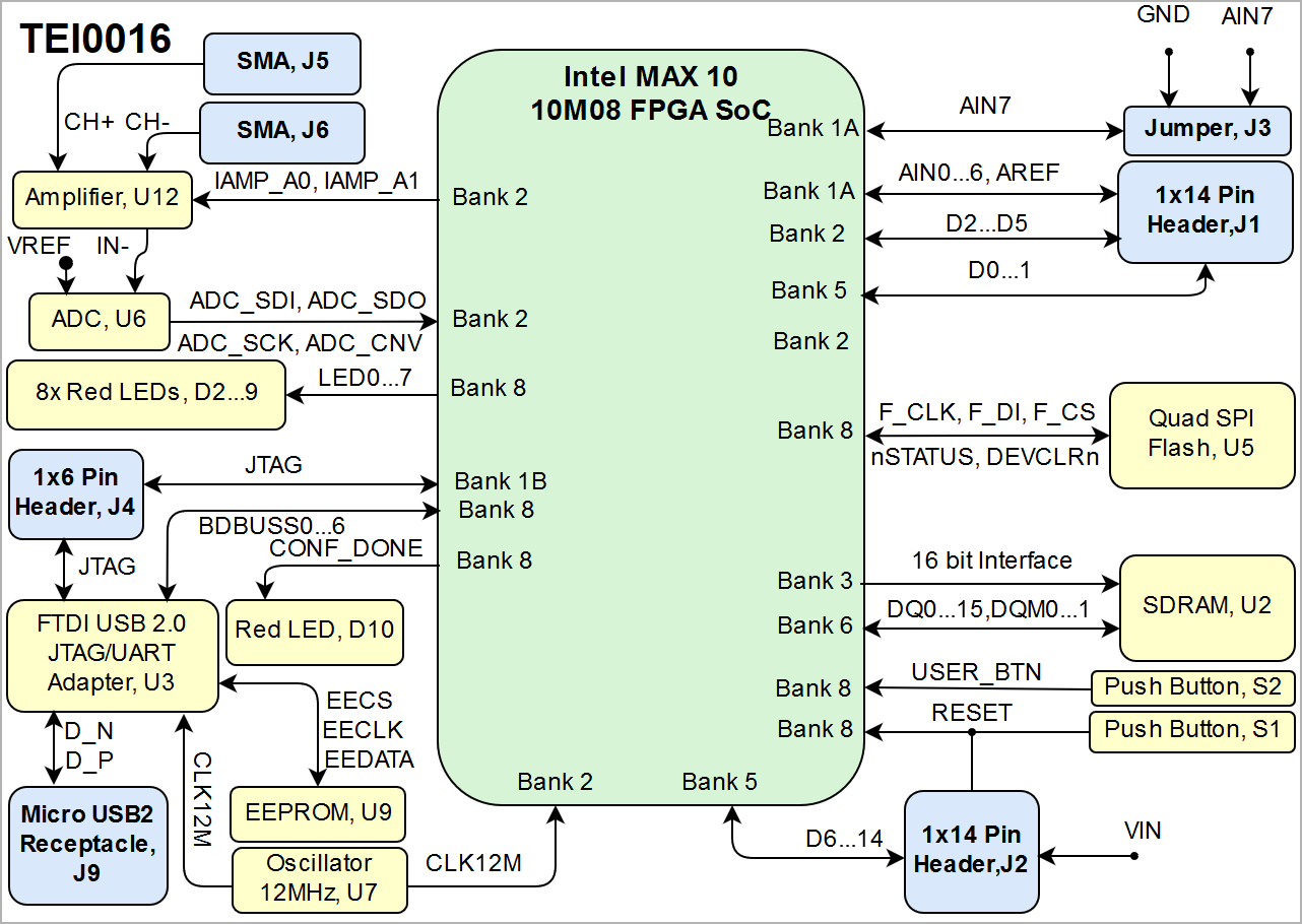
| anchor | Figure_OV_BD |
|---|
| title | TEI0016 block diagram |
|---|
|
| Scroll Ignore |
|---|
| draw.io Diagram |
|---|
| border | false |
|---|
| viewerToolbar | true |
|---|
| |
|---|
| fitWindow | false |
|---|
| diagramDisplayName | |
|---|
| lbox | true |
|---|
| revision | 89 |
|---|
| diagramName | TEI0016_OV_BD |
|---|
| simpleViewer | false |
|---|
| width | |
|---|
| links | auto |
|---|
| tbstyle | hidden |
|---|
| diagramWidth | 641 |
|---|
|
|
| Scroll Only |
|---|
|
|
...
- SMA Connector, J5...6
- Amplifier, U12
- Analog to Digital ConvertorConverter, U6
- Voltage Reference, U8
- Voltage Regulator, U10 - U13 - U16
- Switching Voltage3 Voltage Regulator, U11 - U4
- SDRAM Memory, U2
- Intel® MAX 10, U1
- SPI Flash Memory, U5
- 12.00 MHz MEMS oscillator, U7
- FTDI USB2 to JTAG/UART adapter, U3
- User LEDs, D2...9
- 4Kb EEPROM, U9
- Configuration LED (Red) , D10
- Power-on LED (Green), D1
- Push button, S1...2
- Micro USB2 Receptacle, J9
- 1x14 pin header , J2 (Not assembled), J2
- 1x6 pin header , J4 (Not assembled), J4
- Jumper, J3
- 1x14 pin header , J1 (Not assembled), J1
Initial Delivery State
| Page properties |
|---|
|
Notes : Only components like EEPROM, QSPI flash and DDR3 can be initialized by default at manufacture. If there is no components which might have initial data ( possible on carrier) you must keep the table empty |
...
| Scroll Title |
|---|
| anchor | Table_OBP_USB |
|---|
| title | Micro USB-2 connector pins |
|---|
|
| Scroll Table Layout |
|---|
| orientation | portrait |
|---|
| sortDirection | ASC |
|---|
| repeatTableHeaders | default |
|---|
| style | |
|---|
| widths | |
|---|
| sortByColumn | 1 |
|---|
| sortEnabled | false |
|---|
| cellHighlighting | true |
|---|
|
| Pins | Connected to | Note |
|---|
| VBUS | USB_VBUS | It is connected to GND |
| | D+ | FTDI U3, DP pin |
| | D- | FTDI U3, DM pin |
|
|
...
| Scroll Title |
|---|
| anchor | Table_SIP_JTG |
|---|
| title | JTAG pins connection |
|---|
|
| Scroll Table Layout |
|---|
| orientation | portrait |
|---|
| sortDirection | ASC |
|---|
| repeatTableHeaders | default |
|---|
| style | |
|---|
| widths | |
|---|
| sortByColumn | 1 |
|---|
| sortEnabled | false |
|---|
| cellHighlighting | true |
|---|
|
JTAG Signal | Pin Header Connector | Note |
|---|
| TMS | J4-6 |
| | TDI | J4-5 |
| | TDO | J4-4 |
| | TCK | J4-3 |
| | JTAG_EN | J4-2 | connected Pulled-up to 3.33V. |
|
On-board Peripherals
| Page properties |
|---|
|
Notes : - add subsection for every component which is important for design, for example:
- Two 100 Mbit Ethernet Transciever PHY
- USB PHY
- Programmable Clock Generator
- Oscillators
- eMMCs
- RTC
- FTDI
- ...
- DIP-Switches
- Buttons
- LEDs
|
...
| Scroll Title |
|---|
| anchor | Table_OBP |
|---|
| title | On board peripherals |
|---|
|
| Scroll Table Layout |
|---|
| orientation | portrait |
|---|
| sortDirection | ASC |
|---|
| repeatTableHeaders | default |
|---|
| style | |
|---|
| widths | |
|---|
| sortByColumn | 1 |
|---|
| sortEnabled | false |
|---|
| cellHighlighting | true |
|---|
|
|
...
| Scroll Title |
|---|
| anchor | Table_OBP_LED |
|---|
| title | On-board LEDs |
|---|
|
| Scroll Table Layout |
|---|
| orientation | portrait |
|---|
| sortDirection | ASC |
|---|
| repeatTableHeaders | default |
|---|
| style | |
|---|
| widths | |
|---|
| sortByColumn | 1 |
|---|
| sortEnabled | false |
|---|
| cellHighlighting | true |
|---|
|
| Designator | Color | Connected to | Active Level | Note |
|---|
| D2...9 | Red | LED1...8 | Active High | User LEDs | | D10 | Red | CONF_DONE | Active Low | Configuration DONE LED | | D1 | Green | 3.3V Power Rail | Active High | After power on it will be on. |
|
Push Buttons
| Scroll Title |
|---|
| anchor | Table_OBP_LED |
|---|
| title | On-board Push Buttons |
|---|
|
| Scroll Table Layout |
|---|
| orientation | portrait |
|---|
| sortDirection | ASC |
|---|
| repeatTableHeaders | default |
|---|
| style | |
|---|
| widths | |
|---|
| sortByColumn | 1 |
|---|
| sortEnabled | false |
|---|
| cellHighlighting | true |
|---|
|
| Designator | Connected to | Functionality | Note |
|---|
| S1 | RESET | General reset |
| | S2 | USER_BTN | User push button | Connected to Bank 8. |
|
Clock Sources
| Scroll Title |
|---|
| anchor | Table_OBP_CLK |
|---|
| title | Osillators |
|---|
|
| Scroll Table Layout |
|---|
| orientation | portrait |
|---|
| sortDirection | ASC |
|---|
| repeatTableHeaders | default |
|---|
| style | |
|---|
| widths | |
|---|
| sortByColumn | 1 |
|---|
| sortEnabled | false |
|---|
| cellHighlighting | true |
|---|
|
| Clock Source | Schematic Name | Frequency | Note |
|---|
| Microchip MEMS Oscillator, U7 | CLK12M | 12.00 MHz | Connected to FTDI FT2232 U3, pin 3. Connected to FPGA SoC bank 2, pin H6. |
|
Power and Power-On Sequence
...
| Scroll Title |
|---|
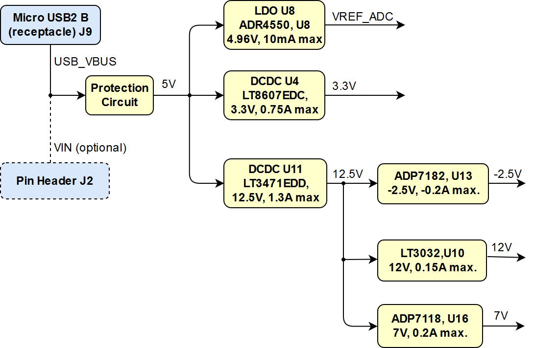
| anchor | Figure_PWR_PD |
|---|
| title | Power Distribution |
|---|
|
| Scroll Ignore |
|---|
| draw.io Diagram |
|---|
| border | false |
|---|
| viewerToolbar | true |
|---|
| |
|---|
| fitWindow | false |
|---|
| diagramDisplayName | |
|---|
| lbox | true |
|---|
| revision | 34 |
|---|
| diagramName | TEI0016_PWR_PD |
|---|
| simpleViewer | false |
|---|
| width | |
|---|
| links | auto |
|---|
| tbstyle | hidden |
|---|
| diagramWidth | 640545 |
|---|
|
|
| Scroll Only |
|---|
|
|
Power-On Sequence
There is no specific or special power-on sequence, just one single power source is needed. After power on, the Green green LED (D1) must be on.
Power Rails
| Scroll Title |
|---|
| anchor | Table_PWR_PR |
|---|
| title | Module power rails. |
|---|
|
| Scroll Table Layout |
|---|
| orientation | portrait |
|---|
| sortDirection | ASC |
|---|
| repeatTableHeaders | default |
|---|
| style | |
|---|
| widths | |
|---|
| sortByColumn | 1 |
|---|
| sortEnabled | false |
|---|
| cellHighlighting | true |
|---|
|
Designator| VCC / VCCIO Schematic Name | VoltageJ2 Pin | Connector J9 Pin | Direction | Notes |
|---|
| VIN | J2-13 |
VIN5V | Input| Input | 5 V - Pin Header | | 3.3V |
3.3V5VJ95V| J9-1 | Input | 5 V - USB Connector |
|
Bank Voltages
| Scroll Title |
|---|
| anchor | Table_PWR_BV |
|---|
| title | Intel Max 10 SoC bank voltages. |
|---|
|
| Scroll Table Layout |
|---|
| orientation | portrait |
|---|
| sortDirection | ASC |
|---|
| repeatTableHeaders | default |
|---|
| style | |
|---|
| widths | |
|---|
| sortByColumn | 1 |
|---|
| sortEnabled | false |
|---|
| cellHighlighting | true |
|---|
|
| Schematic Name | | Notes |
|---|
| Bank 1A | VCCIO1A | 3.3V |
| | Bank 1B | VCCIO1B | 3.3V |
| | Bank 2 | VCCIO2 | 3.3V |
| | Bank 3 | VCCIO3 | 3.3V |
| | Bank 5 | VCCIO5 | 3.3V |
| | Bank 6 | VCCIO6 | 3.3V |
| | Bank 8 | VCCIO8 | 3.3V |
|
|
...
| Scroll Title |
|---|
| anchor | Table_TS_AMR |
|---|
| title | Absolute maximum ratings |
|---|
|
| Scroll Table Layout |
|---|
| orientation | portrait |
|---|
| sortDirection | ASC |
|---|
| repeatTableHeaders | default |
|---|
| style | |
|---|
| widths | |
|---|
| sortByColumn | 1 |
|---|
| sortEnabled | false |
|---|
| cellHighlighting | true |
|---|
|
| Symbols | Description | Min | Max | Unit | Reference Document |
|---|
VIN | Supply voltage | 4.75 | 5.25 | V | | VCC_ONE | Supply voltage for core and periphery through on-die voltage
regulator | -0.5 | 3.9 | V | Intel MAX 10 datasheet | | VCCIO | Supply voltage for input and output buffers | -0.5 | 3.9 | V | Intel MAX 10 datasheet | | VCCA | Supply voltage for phase-locked loop (PLL) regulator and ADC | -0.5 | 3.9 | V | Intel MAX 10 datasheet | | V_AN_IN | Analog Input Voltage on ADC IC U6 pins | -0.1 | 5.1 | V | ADAQ7988B datasheet | | V_REF | Analog reference voltage on IC U6 | -3.2 | 7.7 | V | ADAQ7988B datasheet |
| | CH1-, CH1+ | Analog input voltage on amplifier U12 pin 1, 10 | -30 | 30 | V | AD8251 datasheet | T_STG | Storage Temperature | -40 | CH1+ | Analog input voltage on amplifier U12 pin 10 | 25 | V | AD8251ARMZ datasheet | CH1- | Analog input voltage on amplifier U12 pin 10 | 25 | V | AD8251ARMZ datasheet | T_STG | Storage Temperature | -40 | +85 | °C |
|
|
Recommended Operating Conditions
Operating temperature range depends also on customer design and cooling solution. Please contact us for options.cooling solution. Please contact us for options.
| Scroll Title |
|---|
| anchor | Table_TS_ROC |
|---|
| title | Recommended operating conditions. |
|---|
|
| Scroll Table Layout |
|---|
| orientation | portrait |
|---|
| sortDirection | ASC |
|---|
| repeatTableHeaders | default |
|---|
| style | |
|---|
| widths | |
|---|
| sortByColumn | 1 |
|---|
| sortEnabled | false |
|---|
| cellHighlighting | true |
|---|
|
| Symbols | Min | Max | Unit | Reference Document |
|---|
| VIN supply voltage (5.0V nominal) | 4.75 | 5.25 | V |
| | Analog input voltage on amplifier U12 pin 1 (CH-), 10 (CH+) | -10 | 10 | V |
|
| Scroll Title |
|---|
| anchor | Table_TS_ROC |
|---|
| title | Recommended operating conditions. |
|---|
|
| Scroll Table Layout |
|---|
|
| orientation | portrait |
|---|
| sortDirection | ASC |
|---|
| repeatTableHeaders | default |
|---|
style | widths | | sortByColumn | 1 |
|---|
| sortEnabled | false |
|---|
| cellHighlighting | true |
|---|
| Symbols | Min | Max | Unit | Reference Document |
|---|
VIN supply voltage (5.0V nominal) | 4.75 | 5.25 | V | | VCC_ONE | 3.135 | 3.456 | V | see Intel MAX 10 datasheet |
| VCCIO | 3.135 | 3.456 | V | see Intel MAX 10 datasheet |
| VCCA | 3.135 | 3.456 | V | see Intel MAX 10 datasheet |
| V_AN_IN | 0 | 5 | V | see ADAQ7988B datasheet |
V_REF | 2.4 | 5.1 | V | see ADAQ7988B datasheet |
|
| T_OP | 0 | +70 | °C | W9864G6JT-6 datasheet |
Physical Dimensions
Module size: 86.5 mm × 25 mm. Please download the assembly diagram for exact numbers.
...
| Scroll Title |
|---|
| anchor | Table_RH_DCH |
|---|
| title | Document change history. |
|---|
|
| Scroll Table Layout |
|---|
| orientation | portrait |
|---|
| sortDirection | ASC |
|---|
| repeatTableHeaders | default |
|---|
| style | |
|---|
| widths | |
|---|
| sortByColumn | 1 |
|---|
| sortEnabled | false |
|---|
| cellHighlighting | true |
|---|
|
| Date | Revision | Contributor | Description |
|---|
| Page info |
|---|
| infoType | Modified date |
|---|
| dateFormat | yyyy-MM-dd |
|---|
| type | Flat |
|---|
|
| | Page info |
|---|
| infoType | Current version |
|---|
| prefix | v. |
|---|
| type | Flat |
|---|
| showVersions | false |
|---|
|
| | Page info |
|---|
| infoType | Modified by |
|---|
| type | Flat |
|---|
| showVersions | false |
|---|
|
| | -- | all | | Page info |
|---|
| infoType | Modified users |
|---|
| type | Flat |
|---|
| showVersions | false |
|---|
|
| |
|
...