...
| Scroll Title |
|---|
| anchor | Figure_OV_BD |
|---|
| title | TEI0016 block diagram |
|---|
|
| Scroll Ignore |
|---|
| draw.io Diagram |
|---|
| border | false |
|---|
| viewerToolbar | true |
|---|
| |
|---|
| fitWindow | false |
|---|
| diagramDisplayName | |
|---|
| lbox | true |
|---|
| revision | 913 |
|---|
| diagramName | TEI0016_OV_BD |
|---|
| simpleViewer | false |
|---|
| width | |
|---|
| links | auto |
|---|
| tbstyle | hidden |
|---|
| diagramWidth | 641 |
|---|
|
|
| Scroll Only |
|---|
|
|
...
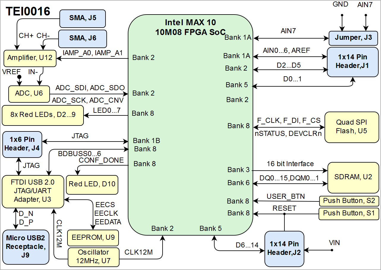
The FPGA configuration for Intel MAX 10 FPGAs can be stored through JTAG interface either in external configuration device (SPI Flash QSPI flash memory U5) or on the FPGA itself since the Intel MAX 10 FPGA offers non-volatile memory on chip. The FPGA configuration is loaded from the non-volatile memory when the board is powered up.
...
| Scroll Title |
|---|
| anchor | Table_OBP_SDRAM |
|---|
| title | SDRAM interface IOs and pins |
|---|
|
| Scroll Table Layout |
|---|
| orientation | portrait |
|---|
| sortDirection | ASC |
|---|
| repeatTableHeaders | default |
|---|
| style | |
|---|
| widths | |
|---|
| sortByColumn | 1 |
|---|
| sortEnabled | false |
|---|
| cellHighlighting | true |
|---|
|
| SDRAM I/O Signals | Signal Schematic Name | Connected to | Notes |
|---|
| Address inputs | A0 ... A13 | bank 3 | - | Bank address inputs
| BA0 / BA1 | bank 3 | - | | Data input/output | DQ0 ... DQ15 | bank 6 | - | | Data mask | DQM0 ... DQM1 | bank 6 | - | | Clock | CLK | bank 3 | - | | Control Signals | CS | bank 3 | Chip select | CKE | bank 3 | Clock enable | RAS | bank 3 | Row Address Strobe | CAS | bank 3 | Column Address Strobe | | WE | bank 3 | Write Enable |
|
...
| Scroll Title |
|---|
| anchor | Table_OBP_LED |
|---|
| title | On-board Push Buttons |
|---|
|
| Scroll Table Layout |
|---|
| orientation | portrait |
|---|
| sortDirection | ASC |
|---|
| repeatTableHeaders | default |
|---|
| style | |
|---|
| widths | |
|---|
| sortByColumn | 1 |
|---|
| sortEnabled | false |
|---|
| cellHighlighting | true |
|---|
|
| Designator | Connected to | Functionality | Note |
|---|
| S1 | RESET | General reset |
| | S2 | USER_BTN | User push button | Connected to FPGA Bank 8. |
|
Clock Sources
| Scroll Title |
|---|
| anchor | Table_OBP_CLK |
|---|
| title | Osillators |
|---|
|
| Scroll Table Layout |
|---|
| orientation | portrait |
|---|
| sortDirection | ASC |
|---|
| repeatTableHeaders | default |
|---|
| style | |
|---|
| widths | |
|---|
| sortByColumn | 1 |
|---|
| sortEnabled | false |
|---|
| cellHighlighting | true |
|---|
|
| Clock Source | Schematic Name | Frequency | Note |
|---|
| Microchip MEMS Oscillator, U7 | CLK12M | 12.00 MHz | Connected to FTDI FT2232 U3, pin 3. Connected to FPGA SoC bank 2, pin H6. |
|
...
| Scroll Title |
|---|
| anchor | Table_TS_ROC |
|---|
| title | Recommended operating conditions. |
|---|
|
| Scroll Table Layout |
|---|
| orientation | portrait |
|---|
| sortDirection | ASC |
|---|
| repeatTableHeaders | default |
|---|
| style | |
|---|
| widths | |
|---|
| sortByColumn | 1 |
|---|
| sortEnabled | false |
|---|
| cellHighlighting | true |
|---|
|
| Symbols | Min | Max | Unit | Reference Document |
|---|
| VIN supply voltage (5.0V nominal) | 4.75 | 5.25 | V |
| | Analog input voltage on amplifier U12 pin 1 (CHCH1-), 10 (CHCH1+) | -10 | 10 | V |
| | T_OP | 0 | +70 | °C | W9864G6JT-6 datasheet |
|
...