| Scroll Table Layout |
|---|
| orientation | portrait |
|---|
| sortDirection | ASC |
|---|
| repeatTableHeaders | default |
|---|
| style | |
|---|
| widths | |
|---|
| sortByColumn | 1 |
|---|
| sortEnabled | false |
|---|
| cellHighlighting | true |
|---|
|
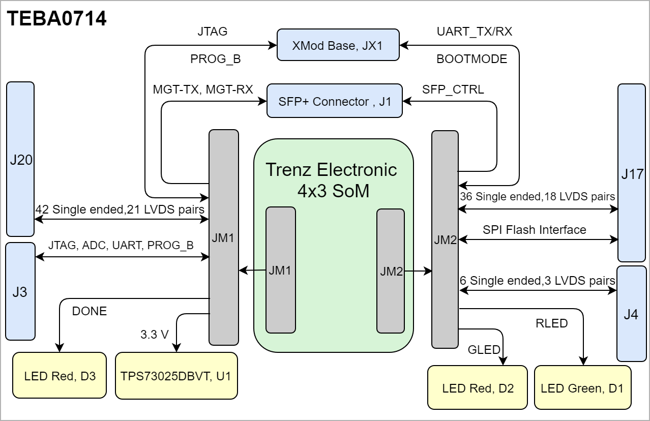
| B2B Connector | I/O Signal Count | Voltage Level | Notes |
|---|
| JM1 | User I/O | 54 single ended or 27 differential | - | | MGT lanes | 4 differential pairs, 2 lanes | - |
| | MGT reference clock input | 1 | - |
| | JTAG | 4 | - |
| | SoM control signals | 2 | 'PROG_B', 'DONE' |
| | ADC interface | 1 differential pair | - |
| | JM2 | User I/O | 36 single ended or 18 differential | - | | SFP+ Interface control signals | 8 | - |
| | QSPI interface | 6 | - |
| | UART interface | 2 | - |
| | User LEDs | 2 | Red, Green |
| | SoM control signals | 1 | 'BOOTMODE' |
|
|