| Page properties |
|---|
|
Template Revision 2.12
- Module: TRM Name always "TE Series Name" +TRM
Example: "TE0728 TRM" - Carrier: TRM Name usually "TEB Series Name" +TRM
Example: "TEB0728 TRM"
|
| HTML |
|---|
<!-- tables have all same width (web max 1200px and pdf full page(640px), flexible width or fix width on menu for single column can be used as before) -->
<style>
.wrapped{
  width: 100% !important;
  max-width: 1200px !important;
 }
</style> |
| Page properties |
|---|
|
Important General Note:
|
| Page properties |
|---|
|
----------------------------------------------------------------------- |
| Page properties |
|---|
|
Note for Download Link of the Scroll ignore macro: |
| Scroll pdf ignore |
|---|
Table of Contents |
Overview
The Trenz Electronic TEBA0714 is a carrier for Trenz Electronic module TE0714 which is an industrial grade module integrated with Xilinx Artix 7.
Refer to http://trenz.org/teba0714-info for the current online version of this manual and other available documentation.
| Page properties |
|---|
|
Notes :- short description of the PCB
- Short Link of the wiki resources reference:
|
Key Features
| Page properties |
|---|
|
Note:
'description: Important components and connector or other Features of the module
→ please sort and indicate assembly optionsKey Features' must be split into 6 main groups:- FPGA/Module
- Package:
- Speed:
- Temperature:
- RAM/Storage
- On Board
- Interface
- E.g. ETH, USB, B2B, Display port
- Power
- E.g. Input supply voltage
- Dimension
|
- Module:
- Trenz TE0714 Module
- Temperature: -40 to +85 °C
- On Board:
- 2 x User LEDs (Red, Green)
- 1 x DONE LED (Red)
- Interface:
- 2 x Pin Header 50 Pol. (FPGA Bank I/Os and Power)
- 2x Samtec 100 Pin LSHM Series Connectors
- 1 x XMOD JTAG/UART Adapter (TE0790)
- 1 x Pin Header 16 Pol. (JTAG, MGT-CLK, Boot Mode, XADC, I/O's)
- 1 x Pin Header 10 Pol. (FPGA Bank I/Os and Power)
- 1 x SFP+ Connectors
- Power:
- 1 x LDO Regulator
- 3.3V Nominal Power supply
- Dimension: 46 mm × 75 mm
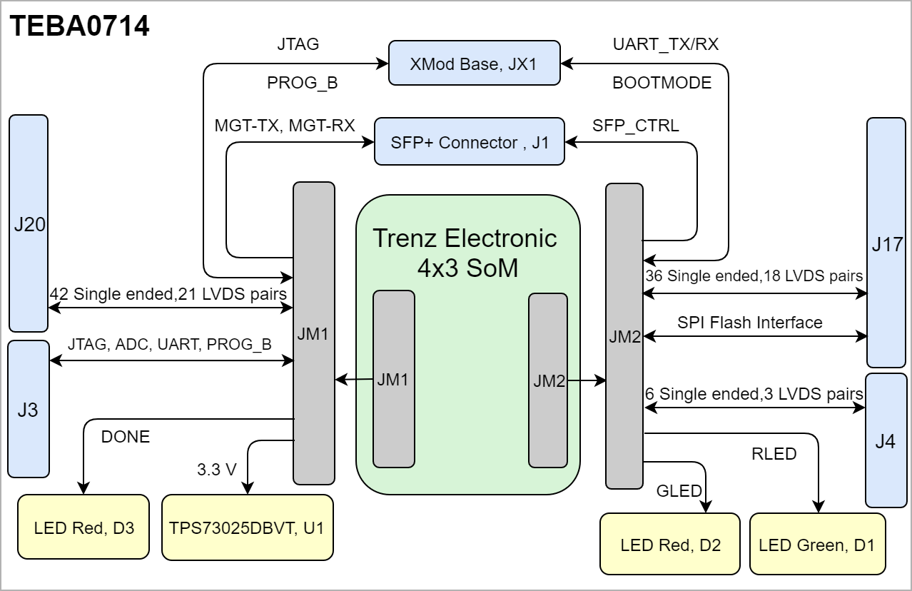
Block Diagram
| Page properties |
|---|
|
add drawIO object here.
|
| Scroll Title |
|---|
| anchor | Figure_OV_BD |
|---|
| title | TEBA0714 block diagram |
|---|
|
| Scroll Ignore |
|---|
| draw.io Diagram |
|---|
| border | false |
|---|
| viewerToolbar | true |
|---|
| |
|---|
| fitWindow | false |
|---|
| diagramDisplayName | |
|---|
| lbox | true |
|---|
| revision | 9 |
|---|
| diagramName | TEBA0714_OV_BD |
|---|
| simpleViewer | false |
|---|
| width | |
|---|
| links | auto |
|---|
| tbstyle | hidden |
|---|
| diagramWidth | 639 |
|---|
|
|
| Scroll Only |
|---|
 |
|
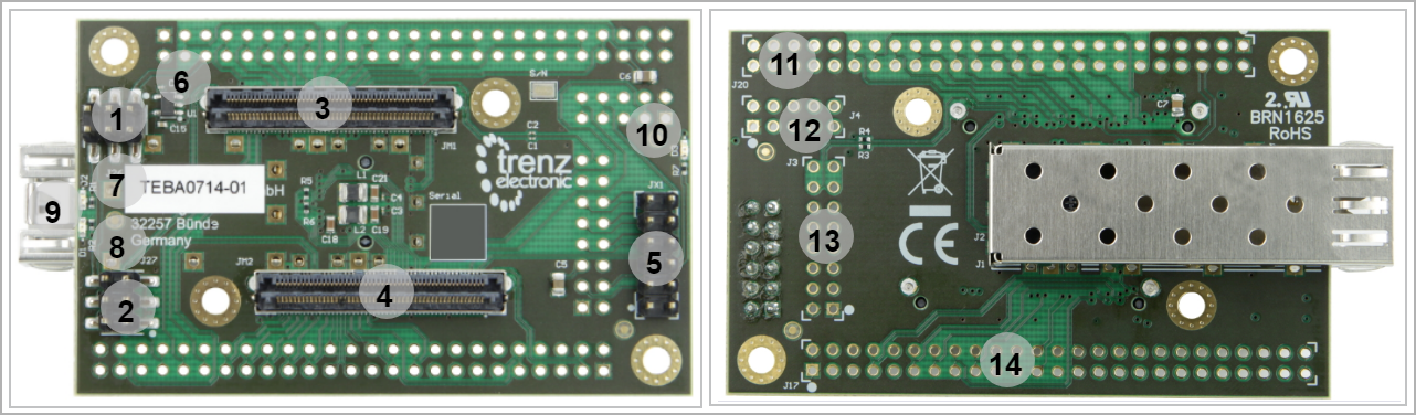
Main Components
| Page properties |
|---|
|
Notes :- Picture of the PCB (top and bottom side) with labels of important components
- Add List below
|
| Scroll Title |
|---|
| anchor | Figure_OV_MC |
|---|
| title | TEBA0714 main components |
|---|
|
| Scroll Ignore |
|---|
| draw.io Diagram |
|---|
| border | false |
|---|
| viewerToolbar | true |
|---|
| |
|---|
| fitWindow | false |
|---|
| diagramDisplayName | |
|---|
| lbox | true |
|---|
| revision | 6 |
|---|
| diagramName | TEBA0714_OV_MC |
|---|
| simpleViewer | false |
|---|
| width | |
|---|
| links | auto |
|---|
| tbstyle | hidden |
|---|
| diagramWidth | 641 |
|---|
|
|
| Scroll Only |
|---|
 |
|
- SMT pin header, J26
- SMT pin header, J27
- Board to Board (B2B) Connector, JM1
- Board to Board (B2B) Connectorr, JM2
- XMOD header, JX1
- Voltage Regulator, U1
- User Red LED, D2
- User Green LED, D1 (Red)
- SFP+ Connector, J1
- User Red LED, D3
- 50-pin header solder pad, J20
- 16-pin header solder pad, J3,
- 10-pin header solder pad, J4
- 50-pin header solder pad, J17
Initial Delivery State
| Page properties |
|---|
|
| Notes :Only components like EEPROM, QSPI flash and DDR3 can be initialized by default at manufacture.If there is no components which might have initial data ( possible on carrier) you must keep the table empty |
- Pin headers (not soldered to the board, but included in the package as separate component)
| Scroll Title |
|---|
| anchor | Table_OV_IDS |
|---|
| title | Initial delivery state of programmable devices on the module |
|---|
|
| Scroll Table Layout |
|---|
| orientation | portrait |
|---|
| sortDirection | ASC |
|---|
| repeatTableHeaders | default |
|---|
| style | |
|---|
| widths | |
|---|
| sortByColumn | 1 |
|---|
| sortEnabled | false |
|---|
| cellHighlighting | true |
|---|
|
| Storage device name | Content | Notes |
|---|
| --- | --- | --- |
|
Configuration Signals
| Page properties |
|---|
|
- Overview of Boot Mode, Reset, Enables.
|
| Scroll Title |
|---|
| anchor | Table_OV_BP |
|---|
| title | Boot process. |
|---|
|
| Scroll Table Layout |
|---|
| orientation | portrait |
|---|
| sortDirection | ASC |
|---|
| repeatTableHeaders | default |
|---|
| style | |
|---|
| widths | |
|---|
| sortByColumn | 1 |
|---|
| sortEnabled | false |
|---|
| cellHighlighting | true |
|---|
|
| Signal | MODE Signal State | Boot Mode | Note |
|---|
| BOOTMODE | 0 | Slave SelectMAP |
| | 1 | Master SPI |
|
|
| Scroll Title |
|---|
| anchor | Table_OV_RST |
|---|
| title | Reset process. |
|---|
|
| Scroll Table Layout |
|---|
| orientation | portrait |
|---|
| sortDirection | ASC |
|---|
| repeatTableHeaders | default |
|---|
| style | |
|---|
| widths | |
|---|
| sortByColumn | 1 |
|---|
| sortEnabled | false |
|---|
| cellHighlighting | true |
|---|
|
| Signal | B2B | Signal State | Note |
|---|
| PROG_B | JM1-94 | Active Low | Clear FPGA configuration vand initiate a new configuration |
|
Signals, Interfaces and Pins
| Page properties |
|---|
|
Notes :- For carrier or stand-alone boards use subsection for every connector type (add designator on description, not on the subsection title), for example:
- For modules which needs carrier use only classes and refer to B2B connector if more than one is used, for example
|
Board to Board (B2B) I/Os
FPGA bank number and number of I/O signals connected to the B2B connector:
| Scroll Title |
|---|
| anchor | Table_SIP_B2B |
|---|
| title | General PL I/O to B2B connectors information |
|---|
|
| Scroll Table Layout |
|---|
| orientation | portrait |
|---|
| sortDirection | ASC |
|---|
| repeatTableHeaders | default |
|---|
| style | |
|---|
| widths | |
|---|
| sortByColumn | 1 |
|---|
| sortEnabled | false |
|---|
| cellHighlighting | true |
|---|
|
| B2B Connector | Interface | Number of I/O | Notes |
|---|
JM1
| User I/O | 52 Single ended, 27 Differential | - | | MGT lanes | 4 Differential, 2 lanes |
| | MGT reference clock input | 2 Single ended, 1 Differential |
| | JTAG | 4 Single ended |
| | SoM control signals | 2 Single ended | 'PROG_B', 'DONE' | | JM2 | User I/O | 36 Single ended or 18 differential | - | | SFP+ Interface control signals | 8 Single ended |
| | QSPI interface | 6 Single ended |
| | UART interface | 2 Single ended |
| | User LEDs | 2 Single ended | Red, Green | | SoM control signals | 1 Single ended | 'BOOTMODE' |
|
| Scroll Title |
|---|
| anchor | Table_SIP_PinHeader |
|---|
| title | General PL I/O to Pin headers information |
|---|
|
| Scroll Table Layout |
|---|
| orientation | portrait |
|---|
| sortDirection | ASC |
|---|
| repeatTableHeaders | default |
|---|
| style | |
|---|
| widths | |
|---|
| sortByColumn | 1 |
|---|
| sortEnabled | false |
|---|
| cellHighlighting | true |
|---|
|
| Pin Header | Interface | Number of I/O | Notes |
|---|
J17
| User I/O | 36 Single ended, 18 Differential | Module FPGA Bank 14 | | SPI interface | 6 Single ended | - | | Power | 4 Single ended | 3.3V, V_CFG | | J20 | User I/O | 42 Single ended or 21 differential | Module FPGA Bank 34 | | Power | 4 Single ended | 3.3V, V_CFG | | User LEDs | 2 Single ended | Red, Green | | SoM control signals | 1 Single ended | 'BOOTMODE' | | J3 | JTAG | 4 Single ended |
| | UART | 2 Single ended | B14_L25, B14_L0 | | ADC | 2 Single ended |
| | Clock | 2 Single ended, 1 Differential |
| | Power | 4 Single ended | 3.3V, V_CFG | | Control Signals | 2 Single ended | BOOTMODE, PROG_B | | J4 | User I/O | 6 Single ended or 3 differential |
| | Power | 2 Single ended | 3.3V, 3.3V_OUT |
|
JTAG Interface Base
JTAG access to the mounted SoM is provided through B2B connector JM1 and JM2 and is also routed to the XMOD JTAG/UART header JX1.
| Scroll Title |
|---|
| anchor | Table_SIP_JTG |
|---|
| title | JTAG pins connection |
|---|
|
| Scroll Table Layout |
|---|
| orientation | portrait |
|---|
| sortDirection | ASC |
|---|
| repeatTableHeaders | default |
|---|
| style | |
|---|
| widths | |
|---|
| sortByColumn | 1 |
|---|
| sortEnabled | false |
|---|
| cellHighlighting | true |
|---|
|
| XMOD Header Pin | B2B Connector | Connected to | Note |
|---|
| A | JM2-97 | B14_L25 | UART Transfer | | B | JM2-99 | B14_L0 | UART Receive | | E | JM2-100 | BOOTMODE |
| | G | JM1-94 | PROG_B |
| | C | JM1-90 | TCK |
| | D | JM1-86 | TDI |
| | F | JM1-88 | TDO |
| | H | JM1-92 | TMS |
| | 3.3V | JM1-97,99 | 3.3V |
| | VIO | JM2-53 | V_CFG |
|
|
SFP+ Connector
| Scroll Title |
|---|
| anchor | Table_SIP_SFP+ |
|---|
| title | SFP+ Connector Information |
|---|
|
| Scroll Table Layout |
|---|
| orientation | portrait |
|---|
| sortDirection | ASC |
|---|
| repeatTableHeaders | default |
|---|
| style | |
|---|
| widths | |
|---|
| sortByColumn | 1 |
|---|
| sortEnabled | false |
|---|
| cellHighlighting | true |
|---|
|
| Pin | Connected to | Notes |
|---|
| VCCR | 3.3V |
| | VCCT | 3.3V |
| | VREF | GND |
| | TD+/TD- | MGT TX | MGT Lane | | RD+/RD- | MGT RX | MGT Lane | | TX/FAULT | SFP0_TX_FAUL | SFP_CTRL | | TX/DISABLE | SFP0_TX_DIS | SFP_CTRL | | MOD-DEF2 | SFP0_SDA | SFP_CTRL | | MOD-DEF1 | SFP0_SCL | SFP_CTRL | | MOD-DEF0 | SFP0_MT_DEF0 | SFP_CTRL | | RS0/RS1 | SFP0_RS0_1 | SFP_CTRL | | LOS | SFP0_LOS | SFP_CTRL |
|
There are two SMT Pin Headers, J26-J27.
J26 is available to choose voltage level for VCCIO34 (FPGA Bank 34) and J27 is provided to set the voltage level of V_CFG (Configuration Voltage). In order to set the voltage level, you should connect it to the corresponding pin with the target value voltage.
| Scroll Title |
|---|
| anchor | Table_SIP_SMD |
|---|
| title | SMD Connector Information |
|---|
|
| Scroll Table Layout |
|---|
| orientation | portrait |
|---|
| sortDirection | ASC |
|---|
| repeatTableHeaders | default |
|---|
| style | |
|---|
| widths | |
|---|
| sortByColumn | 1 |
|---|
| sortEnabled | false |
|---|
| cellHighlighting | true |
|---|
|
| SMT Pin Header | VCCIO/VCC | Voltage Level | Notes |
|---|
| J26 | VCCIO34
| 1.8V |
| | 2.5V |
| | 3.3V_OUT |
| | J27 | V_CFG
| 1.8V |
| | V_CFG0 |
| | 3.3V_OUT |
|
|
On-board Peripherals
| Page properties |
|---|
|
Notes :- add subsection for every component which is important for design, for example:
- Two 100 Mbit Ethernet Transciever PHY
- USB PHY
- Programmable Clock Generator
- Oscillators
- eMMCs
- RTC
- FTDI
- ...
- DIP-Switches
- Buttons
- LEDs
|
| Page properties |
|---|
|
| Notes :In the on-board peripheral table "chip/Interface" must be linked to the corresponding chapter or subsection |
| Scroll Title |
|---|
| anchor | Table_OBP |
|---|
| title | On board peripherals |
|---|
|
| Scroll Table Layout |
|---|
| orientation | portrait |
|---|
| sortDirection | ASC |
|---|
| repeatTableHeaders | default |
|---|
| style | |
|---|
| widths | |
|---|
| sortByColumn | 1 |
|---|
| sortEnabled | false |
|---|
| cellHighlighting | true |
|---|
|
| Chip/Interface | Designator | Notes |
|---|
| LEDs | D1...3 |
|
|
LEDs
| Scroll Title |
|---|
| anchor | Table_OBP_LED |
|---|
| title | On-board LEDs |
|---|
|
| Scroll Table Layout |
|---|
| orientation | portrait |
|---|
| sortDirection | ASC |
|---|
| repeatTableHeaders | default |
|---|
| style | |
|---|
| widths | |
|---|
| sortByColumn | 1 |
|---|
| sortEnabled | false |
|---|
| cellHighlighting | true |
|---|
|
| Designator | Color | Connected to | Active Level | Note |
|---|
| D1 | Green | GLED | Active Low |
| | D2 | Red | RLED | Active High |
| | D3 | Red | DONE | Active High |
|
|
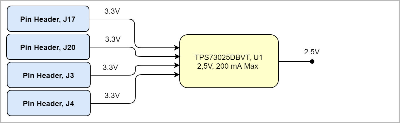
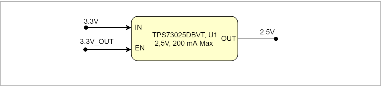
Power and Power-On Sequence
| Page properties |
|---|
|
In 'Power and Power-on Sequence' section there are three important digrams which must be drawn:- Power on-sequence
- Power distribution
- Voltage monitoring circuit
|
Power Supply
Power supply with minimum current capability of 3A for system startup is recommended.
The on-board voltages of the carrier board will be powered up with an external power-supply with nominal voltage of 3.3V.
Power Consumption
| Scroll Title |
|---|
| anchor | Table_PWR_PC |
|---|
| title | Power Consumption |
|---|
|
| Scroll Table Layout |
|---|
| orientation | portrait |
|---|
| sortDirection | ASC |
|---|
| repeatTableHeaders | default |
|---|
| style | |
|---|
| widths | |
|---|
| sortByColumn | 1 |
|---|
| sortEnabled | false |
|---|
| cellHighlighting | true |
|---|
|
| Power Input Pin | Typical Current |
|---|
| VIN | * TBD |
|
* TBD - To Be Determined
Power Distribution Dependencies
| Scroll Title |
|---|
| anchor | Figure_PWR_PD |
|---|
| title | Power Distribution |
|---|
|
| Scroll Ignore |
|---|
| draw.io Diagram |
|---|
| border | false |
|---|
| viewerToolbar | true |
|---|
| |
|---|
| fitWindow | false |
|---|
| diagramDisplayName | |
|---|
| lbox | true |
|---|
| revision | 7 |
|---|
| diagramName | TEBA0714_PWR_PD |
|---|
| simpleViewer | false |
|---|
| width | |
|---|
| links | auto |
|---|
| tbstyle | hidden |
|---|
| diagramWidth | 640 |
|---|
|
|
| Scroll Only |
|---|
 |
|
Power-On Sequence
There is no specific power-on sequence, after power up the module and carrier will be powered on.
| Scroll Title |
|---|
| anchor | Figure_PWR_PS |
|---|
| title | Power Sequency |
|---|
|
| Scroll Ignore |
|---|
| draw.io Diagram |
|---|
| border | false |
|---|
| viewerToolbar | true |
|---|
| |
|---|
| fitWindow | false |
|---|
| diagramDisplayName | |
|---|
| lbox | true |
|---|
| revision | 3 |
|---|
| diagramName | TEBA0714_PWR_PS |
|---|
| simpleViewer | false |
|---|
| width | |
|---|
| links | auto |
|---|
| tbstyle | hidden |
|---|
| diagramWidth | 640 |
|---|
|
|
| Scroll Only |
|---|
 |
|
Power Rails
| Scroll Title |
|---|
| anchor | Table_PWR_PR |
|---|
| title | Module power rails. |
|---|
|
| Scroll Table Layout |
|---|
| orientation | portrait |
|---|
| sortDirection | ASC |
|---|
| repeatTableHeaders | default |
|---|
| style | |
|---|
| widths | |
|---|
| sortByColumn | 1 |
|---|
| sortEnabled | false |
|---|
| cellHighlighting | true |
|---|
|
| Power Rail Name | B2B Connector JM1 Pin | B2B Connector JM2 Pin | Direction | Notes |
|---|
| 3.3V | 99,97 | - | Input |
| | 1.8V | - | 18 | Input |
| | 3.3V_OUT | 83 | 54 | Output |
| | VCCIO34 | 61 | - | Output | Variable voltage level | | V_CFG0 | 53 | - | Input | Variable voltage level |
|
Board to Board Connectors
| Page properties |
|---|
|
- This section is optional and only for modules.
- use "include page" macro and link to the general B2B connector page of the module series,For example: 6 x 6 SoM LSHM B2B Connectors
| Include Page |
|---|
| PD:6 x 6 SoM LSHM B2B Connectors |
|---|
| PD:6 x 6 SoM LSHM B2B Connectors |
|---|
|
|
TEBA0714 carrier use two Samtec Razor Beam LSHM Connectors on the bottom side.
| Include Page |
|---|
| PD:4 x 5 SoM LSHM B2B Connectors |
|---|
| PD:4 x 5 SoM LSHM B2B Connectors |
|---|
|
Technical Specifications
Absolute Maximum Ratings
| Scroll Title |
|---|
| anchor | Table_TS_AMR |
|---|
| title | PS absolute maximum ratings |
|---|
|
| Scroll Table Layout |
|---|
| orientation | portrait |
|---|
| sortDirection | ASC |
|---|
| repeatTableHeaders | default |
|---|
| style | |
|---|
| widths | |
|---|
| sortByColumn | 1 |
|---|
| sortEnabled | false |
|---|
| cellHighlighting | true |
|---|
|
| Symbols | Description | Min | Max | Unit |
|---|
| VIN | Input Supply Voltage | -0.3 | 6 | V | | T_STR | Storage Temperature | -40 | 85 | °C |
|
Recommended Operating Conditions
Operating temperature range depends also on customer design and cooling solution. Please contact us for options.
| Scroll Title |
|---|
| anchor | Table_TS_ROC |
|---|
| title | Recommended operating conditions. |
|---|
|
| Scroll Table Layout |
|---|
| orientation | portrait |
|---|
| sortDirection | ASC |
|---|
| repeatTableHeaders | default |
|---|
| style | |
|---|
| widths | |
|---|
| sortByColumn | 1 |
|---|
| sortEnabled | false |
|---|
| cellHighlighting | true |
|---|
|
| Parameter | Min | Max | Units | Reference Document |
|---|
| VIN | 3.135 | 3.465 | V | 3.3V Nominal Power Supply | | T_OPR | -40 | 85 | °C |
|
|
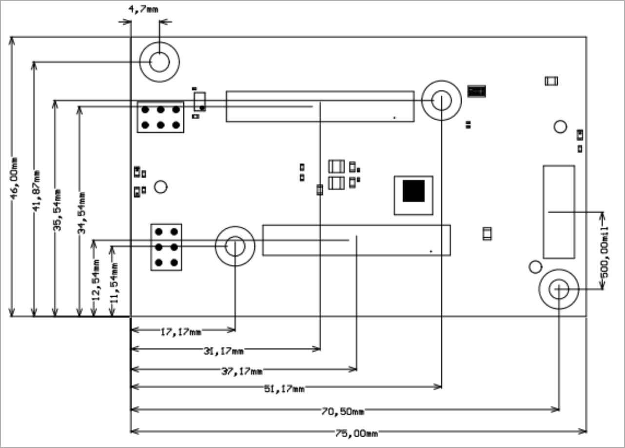
Physical Dimensions
- Module size: 46 mm × 75 mm. Please download the assembly diagram for exact numbers.
- Mating height with standard connectors: 8 mm.
PCB thickness: 1.64 mm.
| Scroll Title |
|---|
| anchor | Figure_TS_PD |
|---|
| title | Physical Dimension |
|---|
|
| Scroll Ignore |
|---|
| draw.io Diagram |
|---|
| border | true |
|---|
| viewerToolbar | true |
|---|
| |
|---|
| fitWindow | false |
|---|
| diagramName | TEBA0714_TS_PD |
|---|
| simpleViewer | false |
|---|
| width | |
|---|
| diagramWidth | 641 |
|---|
| revision | 1 |
|---|
|
|
| Scroll Only |
|---|
| scroll-pdf | true |
|---|
| scroll-office | true |
|---|
| scroll-chm | true |
|---|
| scroll-docbook | true |
|---|
| scroll-eclipsehelp | true |
|---|
| scroll-epub | true |
|---|
| scroll-html | true |
|---|
|  |
|
Currently Offered Variants
| Scroll Title |
|---|
| anchor | Table_VCP_SO |
|---|
| title | Trenz Electronic Shop Overview |
|---|
|
| Scroll Table Layout |
|---|
| orientation | portrait |
|---|
| sortDirection | ASC |
|---|
| repeatTableHeaders | default |
|---|
| style | |
|---|
| widths | |
|---|
| sortByColumn | 1 |
|---|
| sortEnabled | false |
|---|
| cellHighlighting | true |
|---|
|
|
Revision History
Hardware Revision History
| Scroll Title |
|---|
| anchor | Table_RH_HRH |
|---|
| title | Hardware Revision History |
|---|
|
| Scroll Table Layout |
|---|
| orientation | portrait |
|---|
| sortDirection | ASC |
|---|
| repeatTableHeaders | default |
|---|
| style | |
|---|
| widths | |
|---|
| sortByColumn | 1 |
|---|
| sortEnabled | false |
|---|
| cellHighlighting | true |
|---|
|
| Date | Revision | Changes | Documentation Link |
|---|
| 2016-06-15 | 01 | Initial Release | REV01 |
|
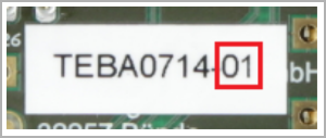
Hardware revision number can be found on the PCB board together with the module model number separated by the dash.
| Scroll Title |
|---|
| anchor | Figure_RV_HRN |
|---|
| title | Board hardware revision number. |
|---|
|
| Scroll Ignore |
|---|
| draw.io Diagram |
|---|
| border | true |
|---|
| viewerToolbar | true |
|---|
| |
|---|
| fitWindow | false |
|---|
| diagramName | Figure_RV_HRN |
|---|
| simpleViewer | false |
|---|
| width | |
|---|
| diagramWidth | 146 |
|---|
| revision | 1 |
|---|
|
|
| Scroll Only |
|---|
 |
|
Document Change History
| Page properties |
|---|
|
- Note this list must be only updated, if the document is online on public doc!
- It's semi automatically, so do following
- Add new row below first
- Copy "Page Information Macro(date)" Macro-Preview, Metadata Version number, Author Name and description to the empty row. Important Revision number must be the same as the Wiki document revision number Update Metadata = "Page Information Macro (current-version)" Preview+1 and add Author and change description. --> this point is will be deleted on newer pdf export template
- Metadata is only used of compatibility of older exports
|
| Scroll Title |
|---|
| anchor | Table_RH_DCH |
|---|
| title | Document change history. |
|---|
|
| Scroll Table Layout |
|---|
| orientation | portrait |
|---|
| sortDirection | ASC |
|---|
| repeatTableHeaders | default |
|---|
| style | |
|---|
| widths | |
|---|
| sortByColumn | 1 |
|---|
| sortEnabled | false |
|---|
| cellHighlighting | true |
|---|
|
| Date | Revision | Contributor | Description |
|---|
| Page info |
|---|
| infoType | Modified date |
|---|
| dateFormat | yyyy-MM-dd |
|---|
| type | Flat |
|---|
|
| | Page info |
|---|
| infoType | Current version |
|---|
| prefix | v. |
|---|
| type | Flat |
|---|
| showVersions | false |
|---|
|
| | Page info |
|---|
| infoType | Modified by |
|---|
| type | Flat |
|---|
| showVersions | false |
|---|
|
| | | -- | all | | Page info |
|---|
| infoType | Modified users |
|---|
| type | Flat |
|---|
| showVersions | false |
|---|
|
| |
|
Disclaimer
| Include Page |
|---|
| IN:Legal Notices |
|---|
| IN:Legal Notices |
|---|
|