...
| Page properties |
|---|
|
Note:
'description: Important components and connector or other Features of the module
→ please sort and indicate assembly options Key Features' must be split into 6 main groups for modules and mainboards: - SoC/FPGA
- Package: SFVC784
- Device: ZU2...ZU5*
- Engine: CG, EG, EV*
- Speed: -1LI, -2LE,*, **
- Temperature: I, E,*, **
- RAM/Storage
- Low Power DDR4 on PS
- Data width: 32bit
- Size: def. 2GB*
- Speed:***
- eMMC
- Data width: 8Bit
- size: def. 8GB *
- QSPI boot Flash in dual parallel mode (size depends on assembly version)
- Data width: 8bit
- size: def. 128MB *
- HyperRAM/Flash (optional, default not assembled)
- MAC address serial EEPROM with EUI-48™ node identity (Microchip 24AA025E48)
- On Board
- Lattice LCMXO2
- PLL SI5338
- Gigabit Ethernet transceiver PHY (Marvell Alaska 88E1512)
- Hi-speed USB2 ULPI transceiver with full OTG support (Microchip USB3320C)
- Interface
- 132 x HP PL I/Os (3 banks)
- ETH
- USB
- 4 GTR (for USB3, Sata, PCIe, DP)
- MIO for UART
- MIO for SD
- MIO for PJTAG
- JTAG
- Ctrl
- Power
- 3.3V-5V Main Input
- 3.3V Controller Input
- Variable Bank IO Power Input
- Dimension
- Notes
- * depends on assembly version
- ** also non low power assembly options possible
- *** depends on used U+ Zynq and DDR4 combination
Key Features' must be split into 6 main groups for carrier: - Modules
- TE0808, TE807, TE0803,...
- RAM/Storage
- On Board
- Interface
- E.g. ETH, USB, B2B, Display port
- Power
- E.g. Input supply voltage
- Dimension
|
- Modules: <Replace for module use "SoC/FPGA" for Carrier "Modules">
- RAM/Storage
- On Board
- Programmable Clock Generator
- I2C Switch IC
- 9x Green LEDs
- 16x RF Transformation
- Reset Push Buttons
- SDIO Port Expander
- DIP Switch...
- Interface
- Power
- Dimension
- Notes
- FL Series Connectors
- 6x SMA Connectors
- Micro USB2.0
- 2x UEC5 Connectors
- 2x UCC8 Connectors
- PCIe 8x Connector
- 2x Samtec Razor Beam SS5 (2x80 pol) Board to Board Connectors
- Power
- Dimension
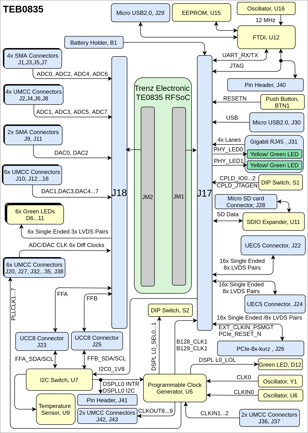
Block Diagram
| Page properties |
|---|
|
add drawIO object here.
|
...
| Scroll Title |
|---|
| anchor | Figure_OV_BD |
|---|
| title | TExxxx block diagram |
|---|
|
| Scroll Ignore |
|---|
| draw.io Diagram |
|---|
| border | truefalse |
|---|
| viewerToolbar | true |
|---|
| |
|---|
| fitWindow | false |
|---|
| diagramDisplayName | |
|---|
| lbox | true |
|---|
| revision | 1 |
|---|
| diagramName | TEB0835_OV_BD |
|---|
| simpleViewer | false |
|---|
| BD | | simpleViewer | false |
|---|
| width | |
|---|
| links | auto |
|---|
| tbstyle | hidden | width |
|---|
| diagramWidth | 641 |
|---|
| revision | 1 |
|---|
|
|
| Scroll Only |
|---|
|
|
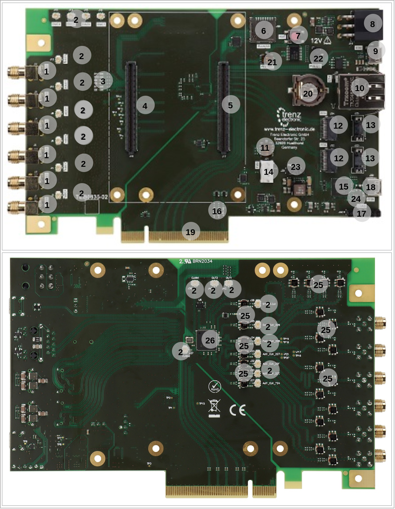
Main Components
...
| Scroll Title |
|---|
| anchor | Figure_OV_MC |
|---|
| title | TEB0835 main components |
|---|
|
| Scroll Ignore |
|---|
| draw.io Diagram |
|---|
| border | truefalse |
|---|
| viewerToolbar | true |
|---|
| |
|---|
| fitWindow | false |
|---|
| diagramDisplayName | |
|---|
| lbox | true |
|---|
| revision | 1 |
|---|
| diagramName | TEB0835_OV_MC |
|---|
| simpleViewer | false |
|---|
| width | |
|---|
| links | auto |
|---|
| tbstyle | hidden |
|---|
| diagramWidth | 641 |
|---|
| revision | 1 |
|---|
|
|
| Scroll Only |
|---|
|
|
- ...
- ...
- ...
Initial Delivery State
...
| Scroll Title |
|---|
| anchor | Table_OV_IDS |
|---|
| title | Initial delivery state of programmable devices on the module |
|---|
|
| Scroll Table Layout |
|---|
| orientation | portrait |
|---|
| sortDirection | ASC |
|---|
| repeatTableHeaders | default |
|---|
| style | |
|---|
| widths | |
|---|
| sortByColumn | 1 |
|---|
| sortEnabled | false |
|---|
| cellHighlighting | true |
|---|
|
Storage device name | Content | Notes |
|---|
| --- | --- | --- |
|
Configuration Signals
| Page properties |
|---|
|
- Overview of Boot Mode, Reset, Enables.
|
...
| Scroll Title |
|---|
| anchor | Table_OV_BP |
|---|
| title | Boot process. |
|---|
|
| Scroll Table Layout |
|---|
| orientation | portrait |
|---|
| sortDirection | ASC |
|---|
| repeatTableHeaders | default |
|---|
| style | |
|---|
| widths | |
|---|
| sortByColumn | 1 |
|---|
| sortEnabled | false |
|---|
| cellHighlighting | true |
|---|
|
MODE Signal State | Boot Mode |
|---|
|
|
|
|
|
| Scroll Title |
|---|
| anchor | Table_OV_RST |
|---|
| title | Reset process. |
|---|
|
| Scroll Table Layout |
|---|
| orientation | portrait |
|---|
| sortDirection | ASC |
|---|
| repeatTableHeaders | default |
|---|
| style | |
|---|
| widths | |
|---|
| sortByColumn | 1 |
|---|
| sortEnabled | false |
|---|
| cellHighlighting | true |
|---|
|
|
...
| Scroll Title |
|---|
| anchor | Table_SIP_B2B |
|---|
| title | General PL I/O to B2B connectors information |
|---|
|
| Scroll Table Layout |
|---|
| orientation | portrait |
|---|
| sortDirection | ASC |
|---|
| repeatTableHeaders | default |
|---|
| style | |
|---|
| widths | |
|---|
| sortByColumn | 1 |
|---|
| sortEnabled | false |
|---|
| cellHighlighting | true |
|---|
|
| FPGA Bank | B2B Connector | I/O Signal Count | Voltage Level | Notes |
|---|
|
|
|
|
|
|
|
|
|
|
|
|
|
|
|
|
|
|
|
|
|
|
|
|
|
|
|
|
|
|
|
JTAG Interface
JTAG access to the TExxxx TEB0835 SoM through B2B connector JMXJM2.
| Scroll Title |
|---|
| anchor | Table_SIP_JTG |
|---|
| title | JTAG pins connection |
|---|
|
| Scroll Table Layout |
|---|
| orientation | portrait |
|---|
| sortDirection | ASC |
|---|
| repeatTableHeaders | default |
|---|
| style | |
|---|
| widths | |
|---|
| sortByColumn | 1 |
|---|
| sortEnabled | false |
|---|
| cellHighlighting | true |
|---|
|
JTAG Signal | B2B Connector |
|---|
| TMS |
| | TDI |
| | TDO |
| | TCK |
| | JTAG_EN |
|
|
MIO Pins
| Page properties |
|---|
|
you must fill the table below with group of MIOs which are connected to a specific components or peripherals, you do not have to specify pins in B2B, Just mention which B2B is connected to MIOs. The rest is clear in the Schematic. Example: | MIO Pin | Connected to | B2B | Notes |
|---|
| MIO12...14 | SPI_CS , SPI_DQ0... SPI_DQ3 SPI_SCK | J2 | QSPI |
|
...
| Scroll Title |
|---|
| anchor | Figure_PWR_PD |
|---|
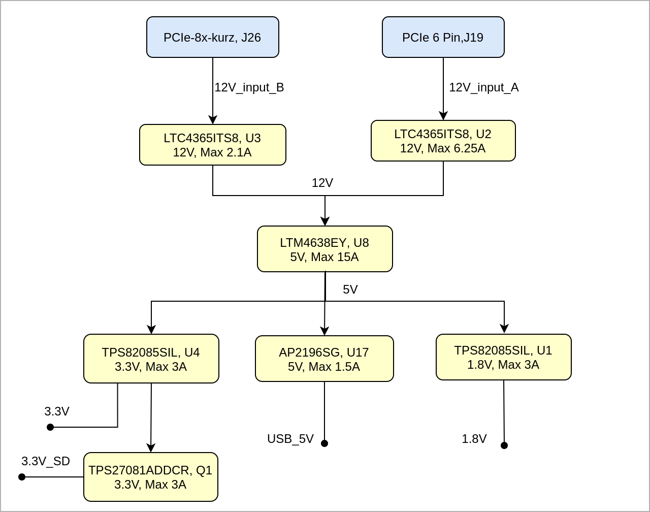
| title | Power Distribution |
|---|
|
| Scroll Ignore |
|---|
| draw.io Diagram |
|---|
| border | truefalse |
|---|
| viewerToolbar | true |
|---|
| |
|---|
| fitWindow | false |
|---|
| diagramDisplayName | |
|---|
| lbox | true |
|---|
| revision | 1 |
|---|
| diagramName | TEB0835_PWR_PD |
|---|
| simpleViewer | false |
|---|
| width | |
|---|
| links | auto |
|---|
| tbstyle | hidden |
|---|
| diagramWidth | 641 | revision | 1 |
|---|
|
|
| Scroll Only |
|---|
|
|
Power-On Sequence
...