...
- SMA Connectors, J1,J3,J5,J7,J9,J11
- U.FL (UMCC) Connectors, J2,J4,J6,J8, J10, J12...16
- Green LEDs, D6...11
- B2B Connector, J18
- B2B Connector, J17
- Micro SD Card Connector, J28
- Reset Push Button, BTN1
- Mosfet Transistors
- PCIe Connector, J19
- Micro USB2.0 Connectors, J29-J30
- Gigabit RJ45 Connector, J31
- DIP Switch, S1
- UEC5 Connector, J22,J24
- UCC8 Connector, J23,J25
- 4x1 Pin Header, J21
- FTDI, U12
- Green LEDs, D1...3
- 4x1 Pin Header, J20
- EEPROM, U15
- PCIe -8x-kurz ConnectorCard, J26
Initial Delivery State
...
| Scroll Title |
|---|
| anchor | Table_OV_RST |
|---|
| title | Reset process. |
|---|
|
| Scroll Table Layout |
|---|
| orientation | portrait |
|---|
| sortDirection | ASC |
|---|
| repeatTableHeaders | default |
|---|
| style | |
|---|
| widths | |
|---|
| sortByColumn | 1 |
|---|
| sortEnabled | false |
|---|
| cellHighlighting | true |
|---|
|
Signal | B2B | I/O | Note |
|---|
RESETN | J17- 36 | Input | Connected to Push Button, BTN1 |
|
Signals, Interfaces and Pins
...
| Scroll Title |
|---|
| anchor | Table_SIP_B2B |
|---|
| title | General PL I/O to B2B connectors information |
|---|
|
| Scroll Table Layout |
|---|
| orientation | portrait |
|---|
| sortDirection | ASC |
|---|
| repeatTableHeaders | default |
|---|
| style | |
|---|
| widths | |
|---|
| sortByColumn | 1 |
|---|
| sortEnabled | false |
|---|
| cellHighlighting | true |
|---|
|
| FPGA Bank | B2B Connector | I/O Signal Count | Voltage Level | Notes |
|---|
|
JTAG Interface
JTAG access to the TEB0835 SoM through B2B connector JM2.
...
| anchor | Table_SIP_JTG |
|---|
| title | JTAG pins connection |
|---|
...
JTAG Signal
...
B2B Connector
...
MIO Pins
...
you must fill the table below with group of MIOs which are connected to a specific components or peripherals, you do not have to specify pins in B2B, Just mention which B2B is connected to MIOs. The rest is clear in the Schematic.
Example:
| Bank 500 | J17 | 12x Single Ended | 1.8V | MIO14...25 | | Bank 501 | J17 | 20x Single Ended | 1.8V | MIO26...51 | | Bank 505 | J17 | 18x Single Ended, 9x Differential pairs | 0.85V | EXT_CLKIN_PSMGT, RX/TX0...3 | | Bank 128 | J17 | 18x Single Ended, 9x Differential pairs | 0.9V | B128_CLK, RX/TX0...3 | | Bank 129 | J17 | 18x Single Ended, 9x Differential pairs | 0.9V | B129_CLK, RX/TX0...3 | | Bank 65 | J18 | 24x Single Ended, 12x Differential pairs | 1.8V |
| | Bank 88 | J18 | 16x Single Ended, 8x Differential pairs | 3.3V | HD_B88 |
|
JTAG Interface
JTAG access to the TEB0835 SoM through B2B connector JM2.
...
SPI_CS , SPI_DQ0... SPI_DQ3
SPI_SCK
...
| anchor | Table_SIP_MIOs |
|---|
| title | MIOs pins |
|---|
...
Test Points
| Page properties |
|---|
|
you must fill the table below with group of Test Point which are indicated as TP in a schematic. If there is no Test Point remarked in the schematic, delet the Test Point section.
Example:
| Test Point | Signal | B2B | Notes |
|---|
10 | PWR_PL_OK | J2-120 | | Scroll Title |
|---|
| anchor | Table_SIP_TPsJTG |
|---|
| title | Test Points InformationJTAG pins connection |
|---|
|
| Scroll Table Layout |
|---|
| orientation | portrait |
|---|
| sortDirection | ASC |
|---|
| repeatTableHeaders | default |
|---|
| style | |
|---|
| widths | |
|---|
| sortByColumn | 1 |
|---|
| sortEnabled | false |
|---|
| cellHighlighting | true |
|---|
|
|
| Test Point | Signal | Connected to | Notes |
|---|
...
JTAG Signal | B2B Connector |
|---|
| TMS |
| | TDI |
| | TDO |
| | TCK |
| | JTAG_EN |
|
|
MIO Pins
| Page properties |
|---|
|
Notes : - add subsection for every component which is important for design, for example:
- Two 100 Mbit Ethernet Transciever PHY
- USB PHY
- Programmable Clock Generator
- Oscillators
- eMMCs
- RTC
- FTDI
- ...
- DIP-Switches
- Buttons
- LEDs
|
you must fill the table below with group of MIOs which are connected to a specific components or peripherals, you do not have to specify pins in B2B, Just mention which B2B is connected to MIOs. The rest is clear in the Schematic. Example: | MIO Pin | Connected to | B2B | Notes |
|---|
| MIO12...14 | SPI_CS , SPI_DQ0... SPI_DQ3 SPI_SCK | J2 | QSPI |
|
| Page properties |
|---|
|
Notes : In the on-board peripheral table "chip/Interface" must be linked to the corresponding chapter or subsection
|
| Scroll Title |
|---|
| anchor | Table_OBPSIP_MIOs |
|---|
| title | On board peripheralsMIOs pins |
|---|
|
| Scroll Table Layout |
|---|
| orientation | portrait |
|---|
| sortDirection | ASC |
|---|
| repeatTableHeaders | default | style | widths |
|---|
| sortByColumn | 1 |
|---|
| sortEnabled | false |
|---|
| cellHighlighting | true |
|---|
|
|
| Chip/Interface | Designator | Notes |
|---|
Quad SPI Flash Memory
| Page properties |
|---|
|
Notes : Minimum and Maximum density of quad SPI flash must be mentioned for other assembly options. |
| | style | |
|---|
| widths | |
|---|
| sortByColumn | 1 |
|---|
| sortEnabled | false |
|---|
| cellHighlighting | true |
|---|
|
| MIO Pin | Connected to | B2B | Notes |
|---|
|
|
|
|
|
|
|
|
|
|
|
|
|
|
|
|
|
|
|
|
|
|
|
|
|
|
|
|
|
|
|
|
|
|
|
|
|
Test Points
| Page properties |
|---|
|
you must fill the table below with group of Test Point which are indicated as TP in a schematic. If there is no Test Point remarked in the schematic, delet the Test Point section. Example: | Test Point | Signal | B2B | Notes |
|---|
| 10 | PWR_PL_OK | J2-120 |
|
|
| Scroll Title |
|---|
| anchor | Table_OBPSIP_SPITPs |
|---|
| title | Quad SPI interface MIOs and pinsTest Points Information |
|---|
|
| Scroll Table Layout |
|---|
| orientation | portrait |
|---|
| sortDirection | ASC |
|---|
| repeatTableHeaders | default |
|---|
| style | |
|---|
| widths | |
|---|
| sortByColumn | 1 |
|---|
| sortEnabled | false |
|---|
| cellHighlighting | true |
|---|
|
|
On-board Peripherals
...
| Page propertiesscroll-title |
|---|
|
Notes : - add subsection for every component which is important for design, for example:
- Two 100 Mbit Ethernet Transciever PHY
- USB PHY
- Programmable Clock Generator
- Oscillators
- eMMCs
- RTC
- FTDI
- ...
- DIP-Switches
- Buttons
- LEDs
|
| Page properties |
|---|
|
Notes : In the on-board peripheral table "chip/Interface" must be linked to the corresponding chapter or subsection |
| anchor | Table_OBP_RTC |
|---|
| title | I2C interface MIOs and pins |
|---|
|
| Scroll Table Layout |
|---|
|
| orientation | portrait |
|---|
| sortDirection | ASC |
|---|
| repeatTableHeaders | default |
|---|
style | widths | | sortByColumn | 1 |
|---|
| sortEnabled | false |
|---|
| cellHighlighting | true |
|---|
MIO Pin | Schematic | U? Pin | Notes
| Scroll Title |
|---|
| anchor | Table_OBP_I2C_RTC |
|---|
| title | I2C Address for RTCOn board peripherals |
|---|
|
| Scroll Table Layout |
|---|
| orientation | portrait |
|---|
| sortDirection | ASC |
|---|
| repeatTableHeaders | default |
|---|
| style | |
|---|
| widths | |
|---|
| sortByColumn | 1 |
|---|
| sortEnabled | false |
|---|
| cellHighlighting | true | true |
|---|
|
|
...
RTC
| Scroll Title |
|---|
| anchor | Table_OBP_EEPRTC |
|---|
| title | I2C EEPROM interface MIOs and pins |
|---|
|
| Scroll Table Layout |
|---|
| orientation | portrait |
|---|
| sortDirection | ASC |
|---|
| repeatTableHeaders | default |
|---|
| style | |
|---|
| widths | |
|---|
| sortByColumn | 1 |
|---|
| sortEnabled | false |
|---|
| cellHighlighting | true |
|---|
|
| MIO Pin | Schematic | U? ? Pin | Notes |
|---|
|
|
|
|
|
|
|
|
|
| Scroll Title |
|---|
| anchor | Table_OBP_I2C_EEPROMRTC |
|---|
| title | I2C address Address for EEPROMRTC |
|---|
|
| Scroll Table Layout |
|---|
| orientation | portrait |
|---|
| sortDirection | ASC |
|---|
| repeatTableHeaders | default |
|---|
| style | |
|---|
| widths | |
|---|
| sortByColumn | 1 |
|---|
| sortEnabled | false |
|---|
| cellHighlighting | true |
|---|
|
| MIO Pin | I2C Address | Designator | Notes |
|---|
|
...
EEPROM
| Scroll Title |
|---|
| anchor | Table_OBP_LEDEEP |
|---|
| title | On-board LEDsI2C EEPROM interface MIOs and pins |
|---|
|
| Scroll Table Layout |
|---|
| orientation | portrait |
|---|
| sortDirection | ASC |
|---|
| repeatTableHeaders | default |
|---|
| style | |
|---|
| widths | |
|---|
| sortByColumn | 1 |
|---|
| sortEnabled | false |
|---|
| cellHighlighting | true |
|---|
|
|
| Designator | Color | Connected to | Active Level | Note |
|---|
DDR3 SDRAM
| Page properties |
|---|
|
Notes : Minimum and Maximum density of DDR3 SDRAM must be mentioned for other assembly options. (pay attention to supported address length for DDR3) |
The TE???? SoM has ??? GByte volatile DDR3 SDRAM IC for storing user application code and data.
- Part number:
- Supply voltage:
- Speed:
- NOR Flash
- Temperature:
...
| MIO Pin | Schematic | U?? Pin | Notes |
|---|
|
|
|
|
|
|
|
|
|
| Scroll Title |
|---|
| anchor | Table_OBP_I2C_EEPROM |
|---|
| title | I2C address for EEPROM |
|---|
|
| Scroll Table Layout |
|---|
| orientation | portrait |
|---|
| sortDirection | ASC |
|---|
| repeatTableHeaders | default |
|---|
| style | |
|---|
| widths | |
|---|
| sortByColumn | 1 |
|---|
| sortEnabled | false |
|---|
| cellHighlighting | true |
|---|
|
| MIO Pin | I2C Address | Designator | Notes |
|---|
|
|
|
|
|
LEDs
| Scroll Title |
|---|
| anchor | Table_OBP_ETHLED |
|---|
| title | Ethernet PHY to Zynq SoC connectionsOn-board LEDs |
|---|
|
| Scroll Table Layout |
|---|
| orientation | portrait |
|---|
| sortDirection | ASC |
|---|
| repeatTableHeaders | default |
|---|
| style | |
|---|
| widths | |
|---|
| sortByColumn | 1 |
|---|
| sortEnabled | false |
|---|
| cellHighlighting | true |
|---|
|
| U?? Pin | Signal NameSignal Description |
...
Ethernet
| Scroll Title |
|---|
| anchor | Table_OBP_CANETH |
|---|
| title | CAN Tranciever interface MIOsEthernet PHY to Zynq SoC connections |
|---|
|
| Scroll Table Layout |
|---|
| orientation | portrait |
|---|
| sortDirection | ASC |
|---|
| repeatTableHeaders | default |
|---|
| style | |
|---|
| widths | |
|---|
| sortByColumn | 1 |
|---|
| sortEnabled | false |
|---|
| cellHighlighting | true |
|---|
|
| Bank | Schematic Pin| Notes | D-Tx | Driver Input | R-Rx | Reciever Output| Signal Name | Connected to | Signal Description | Note |
|---|
|
|
|
|
|
|
|
|
|
|
|
|
|
|
|
|
|
|
|
|
|
|
|
|
|
|
|
|
|
|
|
|
|
|
|
|
|
|
|
|
|
|
|
|
|
|
|
|
|
|
|
|
|
|
|
|
|
|
|
|
|
|
|
|
|
|
|
|
|
|
|---|
Clock Sources
| Scroll Title |
|---|
| anchor | Table_OBP_CLK |
|---|
| title | Osillators |
|---|
|
| Scroll Table Layout |
|---|
| orientation | portrait |
|---|
| sortDirection | ASC |
|---|
| repeatTableHeaders | default |
|---|
| style | |
|---|
| widths | |
|---|
| sortByColumn | 1 |
|---|
| sortEnabled | false |
|---|
| cellHighlighting | true |
|---|
|
| Designator | Description | Frequency | Note |
|---|
|
| MHz |
|
|
| MHz |
|
|
| KHz |
|
|
|
|
|
|
...
| Page properties |
|---|
|
- This section is optional and only for modules.
use "include page" macro and link to the general B2B connector page of the module series, For example: 6 x 6 SoM LSHM B2B Connectors
| Include Page |
|---|
| PD:6 x 6 SoM LSHM B2B Connectors |
|---|
| PD:6 x 6 SoM LSHM B2B Connectors |
|---|
|
|
? x ? modules use two or three Samtec Micro Tiger Eye Connector on the bottom side.
3 x REF-??????? (compatible to ????????), (?? pins, ?? per row)
The TE0835 has two Samtec Razor Beam on the bottom side.
| Include Page |
|---|
| PD:6 x 8 SoM SS5/ST5 B2B Connectors |
|---|
| PD:6 x 8 SoM SS5/ST5 B2B Connectors |
|---|
|
...
Technical Specifications
Absolute Maximum Ratings
| Scroll Title |
|---|
| anchor | Table_TS_AMR |
|---|
| title | PS absolute maximum ratings |
|---|
|
| Scroll Table Layout |
|---|
| orientation | portrait |
|---|
| sortDirection | ASC |
|---|
| repeatTableHeaders | default |
|---|
| style | |
|---|
| widths | |
|---|
| sortByColumn | 1 |
|---|
| sortEnabled | false |
|---|
| cellHighlighting | true |
|---|
|
| Symbols | Description | Min | Max | Unit |
|---|
|
|
|
| V |
|
|
|
| V | V | V | V | V | V | V |
|
|
|
| °C |
|
|
|
| °C |
|
Recommended Operating Conditions
...
Physical Dimensions
Module size: ?? 106.6 mm × ?? 167.7 mm. Please download the assembly diagram for exact numbers.
Mating height with standard connectors: ? 5 mm.
PCB thickness: ?? 1.5 mm.
| Page properties |
|---|
|
In 'Physical Dimension' section, top and bottom view of module must be inserted, information regarding physical dimensions can be obtained through webpage for product in Shop.Trenz, (Download> Documents> Assembly part) for every SoM. For Example: for Module TE0728, Physical Dimension information can be captured by snipping tools from the link below: https://www.trenz-electronic.de/fileadmin/docs/Trenz_Electronic/Modules_and_Module_Carriers/5.2x7.6/TE0745/REV02/Documents/AD-TE0745-02-30-1I.PDF
|
...
| Scroll Title |
|---|
| anchor | Table_RH_HRH |
|---|
| title | Hardware Revision History |
|---|
|
| Scroll Table Layout |
|---|
| orientation | portrait |
|---|
| sortDirection | ASC |
|---|
| repeatTableHeaders | default |
|---|
| style | |
|---|
| widths | |
|---|
| sortByColumn | 1 |
|---|
| sortEnabled | false |
|---|
| cellHighlighting | true |
|---|
|
| Date | Revision | Changes | Documentation Link |
|---|
| 2019-11-29 | REV01 | Initial Release | REV01 |
|
Hardware revision number can be found on the PCB board together with the module model number separated by the dash.
| Scroll Title |
|---|
| anchor | Figure_RV_HRN |
|---|
| title | Board hardware revision number. |
|---|
|
| Scroll Ignore |
|---|
| draw.io Diagram |
|---|
| border | true |
|---|
| viewerToolbar | true |
|---|
| |
|---|
| fitWindow | false |
|---|
| diagramName | TEB0835_RV_HRN |
|---|
| simpleViewer | false |
|---|
| width | |
|---|
| diagramWidth | 641 |
|---|
| revision | 1 |
|---|
|
|
| Scroll Only |
|---|
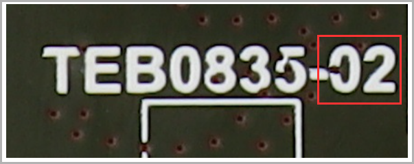 Image Modified Image Modified
|
|
Document Change History
| Page properties |
|---|
|
- Note this list must be only updated, if the document is online on public doc!
- It's semi automatically, so do following
Add new row below first Copy "Page Information Macro(date)" Macro-Preview, Metadata Version number, Author Name and description to the empty row. Important Revision number must be the same as the Wiki document revision number Update Metadata = "Page Information Macro (current-version)" Preview+1 and add Author and change description. --> this point is will be deleted on newer pdf export template - Metadata is only used of compatibility of older exports
|
...