Page History
...
Block Diagram
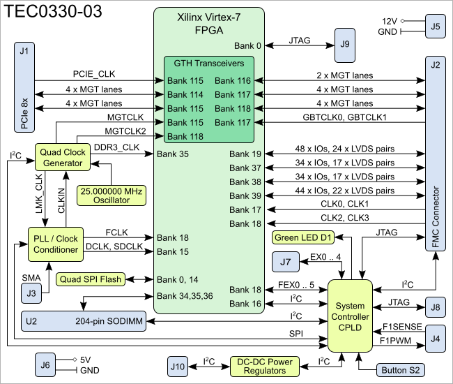
Figure 1: TEC0330-03 Block Diagramblock diagram.
Main Components
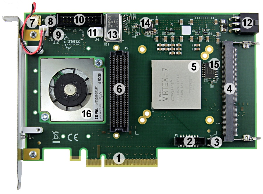
Figure 2: FPGA board TEC0330-03.
...
The I/O signals are routed from the FPGA I/O banks to the FMC connector as LVDS pairs:
| FPGA Bank | I/O Signals | LVDS pairs | Bank Voltage (VCCO) | Notes |
|---|---|---|---|---|
| Bank 19 | 92 | 46 | 1.8V | - |
| Bank 39 | 42 | 21 | VIO_B_FMC | Bank voltage VIO_B_FMC must be supplied by FMC connector pins J2-J39, J2-K40. Bank's VREF_B_M2C signal is routed to the FMC connector pin J2-K1 (external reference voltage). |
| Bank 37 | 34 | 17 | 1.8V | Bank's VREF_A_M2C signal is routed to the FMC connector pin J2-H1 (external reference voltage). |
| Bank 38 | 34 | 17 | 1.8V | Bank's VREF_A_M2C signal is routed to the FMC connector pin J2-H1 (external reference voltage). |
Table 2: Overview of the FPGA I/O bank signals routed to the FMC.
...
There are also 10 high-speed MGT lanes (Xilinx GTH transceivers) from different FPGA MGT banks routed to the FMC connector. The MGT banks have also clock input pins which are exposed to the FMC connector. Following MGT lanes are available on the FMC connector:
| FPGA Bank | I/O signalsSignals | LVDS pairsPairs | MGT lanesLanes | MGT Bank's reference clock (LVDS pair)Reference Clock |
|---|---|---|---|---|
| 116 | 108 | 54 | 2 | 1 clock-signal from clock synthesizer U9 to bank's pins T6/T5 |
| 117 | 2016 | 108 | 4 | 2 clock-signals from clock FMC connector GBTCLK0_M2C and GBTCLK1_M2C (pins J2-D4/J2-D5 and J2-B20/J2-B21) to bank's pins M6/M5 and P6/P5 |
| 118 | 2016 | 108 | 4 | 1 reference clock from clock synthesizer U9 to bank's pins F6/F5 1 reference clock from programmable quad clock generator U13 to bank's pins H6/H5 |
Table 3: Overview of MGT banks lanes routed to the FMC connector.
The FMC connector has also two reference clock input pairs (LVDS) routed to the FPGA MGT bank 117, see also section MGT lanes.
| Page break |
|---|
The FMC connector provides JTAG and There are also JTAG, I2C interfaces to the interface and power good control signals routed between FMC connector and System Controller CPLD:
| Interface | I/O |
|---|
| Signals | Schematic |
|---|
| Name / FMC |
|---|
| Pin | Connected to | Notes | ||
|---|---|---|---|---|
| JTAG | 5 | FMC_TRST, pin D34 FMC_TCK, pin D29 FMC_TMS, pin D33 FMC_TDI, pin D30 FMC_TDO, pin D31 | SC CPLD, bank 2 | VCCIO: 3V3PCI |
| I2C | 2 | FMC_SCL, pin C30 FMC_SDA, pin C31 | SC CPLD, bank 2 | VCCIO: 3V3PCI I2C-lines 3V3PCI pulled-up |
| Control lines | 3 | FMC_PRSNT_M2C_L, pin H2 FMC_PG_C2M, pin D1 (3V3FMC pull-up) FMC_PG_M2C, pin F1 (3V3FMC pull-up) | SC CPLD, bank 1 | PG - Power Good signal C2M - carrier to mezzanine module M2C - mezzanine module to carrier Internal System Controller CPLD signal assignment: FEX_0_N <= FMC_PG_M2C FMC_PG_C2M <= FMC_PRSNT_M2C_L |
Table 4: FMC connector pin-outs of available interfaces to the System Controller CPLD.
...
Overview
Content Tools