Page History
...
Block Diagram
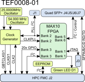
Figure 1: TEF0008 -01 block diagram.
Main Components
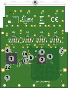
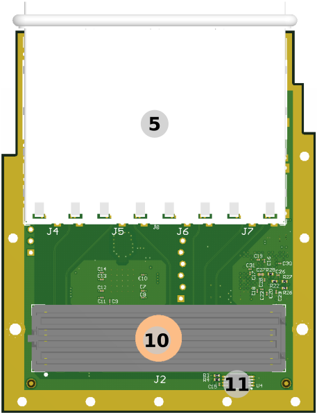
Figure 2: TEF0008 -01 FMC overview.
Table 1: TEF0008 -01 main components.
- MAX10 FPGA, U5
- Programmable low jitter clock generator Si5354A, U2
- Status LED (green), D1
- 3.3V to 1.8V DCDC converter, U6
- Quad SFP+ cage and connectors, J4-J7
- 1x6 pin header for JTAG programming of FPGA (3.3V), J3
- 1x3 pin header for I²C (1.8V), J1
- XTAL 54.0000 MHz (CX3225SB), Y1
- Oszillator 25.000000 MHz (SiT8008B), U1
- HPC FMC connector, J2
- 128KBit EEPROM, U4
- Testpoints Max10, TP7-TP9
- Testpoints JTAG, TP1-TP4
- Testpoints Power, TP5, TP6, TP10
...
Table 7: I2C slave device addresses.
On-board Peripherals
| HTML |
|---|
<!--
Components on the Module, like Flash, PLL, PHY...
--> |
MAX10 FPGA
HPC FMC Connector
The following table lists all on the FMC connector assigned net names.
| A | B | C | D | E | F | G | H | J | K | |
|---|---|---|---|---|---|---|---|---|---|---|
| 1 | GND | NetJ2_B1 | GND | PG_C2M | GND | PG_M2C | GND | GND | ||
| 2 | SFPB_RD_P | GND | SFPA_TD_P | GND | GND | CLK1_P | GND | GND | ||
| 3 | SFPB_RD_N | GND | SFPA_TD_N | GND | GND | CLK1_N | GND | GND | ||
| 4 | GND | GND | GBTCLK0_P | GND | GND | CLK0_P | GND | CLK2_P | ||
| 5 | GND | GND | GBTCLK0_N | GND | GND | CLK0_N | GND | CLK2_N | ||
| 6 | SFPC_RD_P | GND | SFPA_RD_P | GND | GND | LA00_P | GND | GND | ||
| 7 | SFPC_RD_N | GND | SFPA_RD_N | GND | LA00_N | LA02_P | ||||
| 8 | GND | GND | LA01_P | GND | GND | LA02_N | GND | |||
| 9 | GND | GND | LA01_N | GND | LA03_P | GND | GND | |||
| 10 | SFPD_RD_P | GND | LA06_P | GND | LA03_N | LA04_P | ||||
| 11 | SFPD_RD_N | GND | LA06_N | LA05_P | GND | GND | LA04_N | GND | ||
| 12 | GND | GND | LA05_N | GND | LA08_P | GND | GND | |||
| 13 | GND | GND | GND | LA08_N | LA07_P | |||||
| 14 | GND | LA09_P | GND | GND | LA07_N | GND | ||||
| 15 | GND | LA09_N | GND | GND | GND | |||||
| 16 | GND | GND | GND | |||||||
| 17 | GND | GND | GND | GND | GND | |||||
| 18 | GND | GND | GND | GND | ||||||
| 19 | GND | GND | ||||||||
| 20 | GND | GBTCLK1_P | GND | GND | GND | GND | ||||
| 21 | GND | GBTCLK1_N | GND | GND | GND | GND | ||||
| 22 | SFPB_TD_P | GND | GND | |||||||
| 23 | SFPB_TD_N | GND | GND | GND | GND | |||||
| 24 | GND | GND | GND | GND | GND | |||||
| 25 | GND | GND | GND | |||||||
| 26 | SFPC_TD_P | GND | GND | GND | GND | |||||
| 27 | SFPC_TD_N | GND | GND | GND | GND | |||||
| 28 | GND | GND | GND | |||||||
| 29 | GND | GND | TCK | GND | GND | GND | ||||
| 30 | SFPD_TD_P | GND | FMC_SCL | TDI | GND | GND | GND | |||
| 31 | SFPD_TD_N | GND | FMC_SDA | TDO | ||||||
| 32 | GND | GND | 3P3VAUX | GND | GND | GND | ||||
| 33 | GND | GND | TMS | GND | GND | GND | ||||
| 34 | GND | GA0 | ||||||||
| 35 | GND | 12V | GA1 | GND | GND | GND | ||||
| 36 | GND | GND | 3P3V | GND | GND | GND | ||||
| 37 | GND | 12V | GND | |||||||
| 38 | GND | GND | 3P3V | GND | GND | GND | ||||
| 39 | GND | 3P3V | GND | VADJ | GND | VADJ | GND | GND | ||
| 40 | GND | GND | 3P3V | GND | VADJ | GND | VADJ | GND |
Table 8: HPC FMC Connector pin assignment.
On-board Peripherals
| HTML |
|---|
<!--
Components on the Module, like Flash, PLL, PHY...
--> |
MAX10 FPGA
The MAX10 FPGA The MAX10 FPGA (10M08SAU169C8G) is used as SFP control, level shifter and I2C MUX. For a detailed description see TEF0008 MAX10.
...
| Si5345A Pin | Signal Name / Description | Connected To | Direction | Note |
|---|---|---|---|---|
IN0 | Reference input clock. | U1 | Input | 25.000000 MHz oscillator, Si8208AI |
| IN1 | - | Not connected. | Input | Not used. |
IN2 | - | Not connected. | Input | Not used. |
IN3 | CLK2 | J2-K4/K5 | Input | HPC FMC configured as C2M clock. |
A1 | - | GND | Input | I2C slave device address LSB. |
| XAXB | - | Y1 | Input | 54.0000 MHz XTAL CX3225SB |
OUT0 | CLKPLL2F | U5-H6/G5 | Output | FPGA bank 2. |
| OUT1 | - | Not connected. | Output | Not used. |
| OUT2 | GBTCLK1 | J2-B20/B21 | Output | M2C via HPC FMC. |
| OUT3 | - | Not connected. | Output | Not used. |
| OUT4 | - | Not connected. | Output | Not used. |
| OUT5 | - | Not connected. | Output | Not used. |
| OUT6 | - | Not connected. | Output | Not used. |
| OUT7 | GBTCLK0 | J2-D4/D5 | Output | M2C via HPC FMC. |
| OUT8 | CLK0 | J2-H4/H5 | Output | M2C via HPC FMC. |
| OUT9 | CLK1 | J2-G2/G3 | Output | M2C via HPC FMC. |
Table 89: Programmable clock generator inputs and outputs.
...
| Clock Source | Schematic Name | Frequency | Clock Destination |
|---|---|---|---|
| SiTime SiT8008AI oscillator, U1 | - | 25.000000 MHz | U2-63/64 |
| Carrier board via HPC FMC J2-K4/K5 | CLK2 | Defined by carrier. | U2-61/62 |
Table 910: Reference clock signals.
...
| LED | Color | Connected to | Description and Notes |
|---|---|---|---|
| D1 | Green | U5-C2 (bank 1A) | Depending on FPGA design. With the shipped FPGA design it is on, if at least one SFP is connected. |
Table 1011: On-board LED.
Power and Power-On Sequence
...
| 3P3V | TBD* |
| VADJ (at 1.8V) | TBD* |
3P3VAUX | TBD* |
Table 1112: Typical power consumption.
...
Power Rail Name | HPC FMC Connector (J2) | Direction | Notes |
|---|---|---|---|
| 3P3V | D36, D38, D40, C39 | Input | Supply voltage from carrier board. |
| 1.8V | - | Output | Module on-board 1.8V voltage supply (Max 1A). |
3P3VAUX | D32 | Input | Supply voltage from carrier board. |
VADJ | H40, G39, F40, E39 | Input | Supply voltage from carrier board. |
| 12V | C35, C37 | Input | Not used supply voltage from carrier board. |
Table 1213: Module power rails.
Bank Voltages
Bank | Schematic Name | Voltage | Voltage Range |
|---|---|---|---|
| 1A | 3P3V | 3.3V | - |
| 1B | 3P3V | 3.3V | - |
| 2 | 1.8V | 1.8V | - |
| 3 | VADJ | Carrier supplied | 1.2V - 3.3V |
| 5 | 3P3V | 3.3V | - |
| 6 | 3P3V | 3.3V | - |
| 8 | 3P3V | 3.3V | - |
Table 1314: Module PL I/O bank voltages.
...
| Module Variant | FPGA | Operating Temperature | Temperature Range |
|---|---|---|---|
| TE0008-0102 | 10M08SAU169C8G | 0°C to +85°C | Extended |
Table 1415: Module variants.
Technical Specifications
...
Parameter | Min | Max | Units | Reference Document |
|---|---|---|---|---|
Storage temperature | -40 | 85 | °C | - |
Table 1516: Module absolute maximum ratings.
...
| Date | Revision | Notes | PCN | Documentation Link |
|---|---|---|---|---|
| 2018-06-06 | 02 | First production release | ||
| - | 01 | Prototypes |
Table 1617: Module hardware revision history.
...
| HTML |
|---|
<!-- Generate new entry: 1.add new row below first 2.Copy "Page Information Macro(date)" Macro-Preview, Metadata Version number, Author Name and description to the empty row. Important Revision number must be the same as the Wiki document revision number 3.Update Metadata = "Page Information Macro (current-version)" Preview+1 and add Author and change description. --> |
Date | Revision | Contributors | Description |
|---|---|---|---|
|
|
|
| Martin Rohrmüller | Updated Table 15 and 17 to Rev02. Added FMC connector pin assignment (Table 8). | ||||
Martin Rohrmüller | Initial document. | |||||
all | Jan Kumann, John Hartfiel |
Table 1718: Document change history.
...
Overview
Content Tools