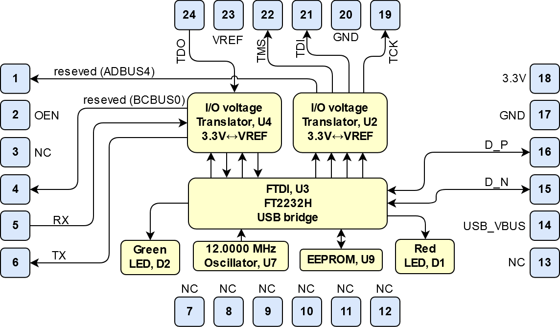
| Pin Designator | Signal | Module Direction |
|---|
| 1 | reserved for future use | out |
| 2 | OEN (enable data transmitting), low active | in |
| 3 | Do not connect (reserved for future use) | - |
| 4 | reserved for future use | out |
| 5 | UART RX | in |
| 6 | UART TX | out |
| 7...13 | Do not connect (reserved for future use) | - |
| 14 | USB-VBUS (USB Host supply voltage) | in |
| 15 | USB Data - | bidir |
| 16 | USB Data + |
| 17 | GND | - |
| 18 | 3.3V output voltage from module | out |
| 19 | TCK | out |
| 20 | GND | - |
| 21 | TDI | out |
| 22 | TMS | out |
| 23 | VREF (Reference I/O-voltage from target board for JTAG and UART) | in |
| 24 | TDO | in |