Page History
Power Supply Range
TE0320 requires only one power supply with a supply voltage between 4.0 V and 7.0 V. Power consumption depends on the active design.
Power Supply Sources
TE0320 can be power supplied in two ways:
...
| Scroll pdf title | ||
|---|---|---|
| ||
|

1.2 V, 2.5 V and 3.3 V voltage rails are provided by corresponding step-down regulator DC/DC converters, each one capable of providing up to 3 A of output current. These three regulators are synchronized to switch with 120° phase lag, to improve EMC, and to reduce input ripple. The synchronization circuit can be omitted in cost sensitive applications (please contact Trenz Electronic).
Power supply inputs and outputs are made available at B2B connectors JM4 and JM5 for user applications.
| Warning |
|---|
Each pin of B2B connectors JM4 and JM5 is capable of a maximum current of 1.0 A. |
...
| Scroll pdf title | |||||||||||||||||||||||||||||||||||||||||||||||||||||||||||||||||||||||||
|---|---|---|---|---|---|---|---|---|---|---|---|---|---|---|---|---|---|---|---|---|---|---|---|---|---|---|---|---|---|---|---|---|---|---|---|---|---|---|---|---|---|---|---|---|---|---|---|---|---|---|---|---|---|---|---|---|---|---|---|---|---|---|---|---|---|---|---|---|---|---|---|---|---|
| |||||||||||||||||||||||||||||||||||||||||||||||||||||||||||||||||||||||||
|
If resistors R9 and R11 are populated and R12 is not populated, then TE0320 is power supplied through JM5 (B2B connector).
| Scroll pdf title | ||
|---|---|---|
| ||
|

If resistors R9 and R11 are not populated and R12 is populated, then TE0320 is power supplied through J1 (USB bus).
| Scroll pdf title | ||
|---|---|---|
| ||
|

| Warning |
|---|
Any other assembly combination of R9, R11 and R12 is not allowed. |
On Board Power Rails
According to the Xilinx Spartan-3A DSP literature, there are the following power supply pin types:
...
if inductor L2 is not populated and the low-noise low drop-out regulator U6 is populated, VCCAUX power rail is supplied with its nominal voltage of 2.5 V. This is the recommended option for noise-sensitive circuitry such as clocking and timing infrastructures.
Scroll pdf title title Assembly option for VCCAUX = 2.5 V (bottom view). 
- if the ferrite bead L2 is populated and U6 is not populated, the 3.3V power rail is simply filtered to generate VCCAUX power rail. This is the recommended option for cost-sensitive applications. In this case
- ensure the noise level on power rail VCCUAX is suitable to your application;
avoid the connection of noise sources to power rail VCCUAX.
Scroll pdf title title Assembly option for VCCAUX = 3.3 V (bottom view). 
Warning Any other assembly combination of L2 and U6 is not allowed.
...
if resistor R131 is not populated and R132 is populated, VCCCIO0 power rail is set to power rail 2.5V (nominal voltage = 2.5 V).
Scroll pdf title title Assembly option for VCCIO0= 2.5 V (bottom view). 
Note Pins 30 and 44 of JM4 are power supply inputs in this case.
if resistor R131 is populated and R132 is not populated, VCCCIO0 power rail is set to power rail 3.3V (nominal voltage = 3.3 V). This is the default.
Scroll pdf title title Assembly option for VCCCIO0 = 3.3 V (bottom view). 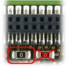
Note Pins 30 and 44 of JM4 are power supply outputs in this case.
if both resistors R131 and R132 are not populated, VCCCIO0 power can be supplied through pins 30 and 44 of B2B connector JM4.
Scroll pdf title title Assembly option for VCCAUX = off (bottom view) 
Note Pins 30 and 44 of JM4 are power supply outputs in this case.
Warning Assembly option where both R131 and R132 are populated is not allowed.
Power Supervision
Power-on Reset
During power-on, the /RESET line is first asserted. Thereafter, the supply voltage supervisor monitors the power supply rail 3.3V and keeps the /RESET line active (low) as long as the rail remains below the threshold voltage (2.93 V). An internal timer delays the return of the /RESET line to the inactive state (high) to ensure proper system reset. The delay time of 200 ms starts after the rail has risen above the threshold voltage.
| Scroll pdf title | ||
|---|---|---|
| ||
|

After this delay, the /RESET line is reset high and the FPGA configuration can start.
...
| Scroll pdf title | ||
|---|---|---|
| ||
|

Power-on Reset
TE0320 integrates a power-fail comparator which can be used for low-battery detection, power-fail warning, or for monitoring Vsup power rail.
...
Overview
Content Tools