Page History
...
Port D Pin | Alternate Function | Alternate Function is Selected By... | Alternate Function is Described in... |
|---|---|---|---|
| PD.7:0 | FD[15:8] | IFCFG1 = 1 and any WORDWIIDE bit = 1 | Slave FIFOs chapter 9 on page 99 |
Table from EZ-USB(R) Technical Reference Manual (EZ-USB_TRM.pdf).
Signal PS_EN
- Signal PS_EN enables (1) or disables (0) power rails 2.5V and 1.2V.

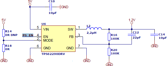
Figure 36: Power rails 2.5V and 1.2V could be enabled/disabled by signal PS_EN. Power-rail 3.3V is not controlled by signal PS_EN and is unconditionally enabled.

Figure 37: Power rails 3.3V could not be enabled/disabled by signal PS_EN.
The 3.3 V power-rail though is out of the control of the USB-microcontroller and is supplied down-converting the 5 V power supply provided by either the USB-bus or the B2B receptacle connector. In this case, signals that are applied to the 3.3 V I/O banks do not need to be disconnected when power-rails are disabled by the USB microcontroller.
VCCIO0 assembly options
According to the corresponding assembly option, power rail VCCCIO0 can depend or not on the 2.5V power rail.
Voltage VccIO for bank B0 shall span from 1.2 V to 3.3 V. VccIO can be supplied either externally or internally to the micromodule.
| Warning! Spartan-3 I/Os are not 5 V tolerant. Applying more than the recommended operating voltages at any pin, results in a damaged FPGA (see Xilinx Answer AR#19146). |
|---|
Externally Supplied
VccIOVCCIO
VccIO can be externally supplied over the B2B connector J4. If bank B0 is not used, then VccIO can be left open.
Internally Supplied
VccIOVCCIO
If VccIO is not externally supplied, it can be internally supplied by one of the internal power rails of 2.5 V and 3.3 V. This is possible by short-circuiting one of the two pad pairs placed on the right of connector J4 at the top right corner of the bottom side of the micromodule.
Two suitable ways of shirt-circuiting the paid pair are by means of a zero-ohm 0603 (1608 metric) chip resistor or a solder blob.


Figure 37: example of VCCIO0 assembly not dependent on 2. 5V power rail. The other way is also possible The soldering of R102 and R103 are mutually exclusive.

Figure 9 shows how to short-circuit VccIO to internal 3.3 V power rail. FX2_PS_EN does not control VCCCIO0 (3.3V) FPGA bank 0

Figure 10 shows how to short-circuit VccIO to internal 2.5 V power rail. FX2_PS_EN does control VCCCIO0 (2.5V) FPGA bank 0
Slide Switch S3 = FX2 PON
...
- Dynamic full power operation (PS_EN = 1): when the EZ-USB FX2LP USB FX2 microcontroller sets signal PS_EN = FX2_PS_EN = 1, power rails 2.5V and 1.2V are enabled.
This setting can be useful for . - Dynamic low power operation (PS_EN = 0): when the EZ-USB FX2LP USB FX2 microcontroller resets signal PS_EN = FX2_PS_EN = 0, the following components are switched off:
FPGA core logic (1.2V)DDR SDRAM (2.5V)- FPGA bank 3 1 (2.5V)
VREF (2.5V)VCCCIO0 (2.5V) FPGA bank 0 (if R102+R103- assembly)
Slide Switch S3 = PON
Full power operation (PS_EN = 1): when slide switch S3 is in the right position (PON = power rails unconditionally on), signal PS_EN is set to power rail 3.3V. Thus power rails 2.5V and 1.2V are unconditionally enabled.


Figure 39: S3 on position PON (PS_EN ≠ FX2_PS_EN = x; PS_EN = high ).
...
power rail | S3= PON | S3 = FX2 PON and | S3 = FX2 PON and |
|---|---|---|---|
1.2V | on | on | off |
2.5V | on | on | off |
VCCCIO0 (= 2.5V) | on | on | off |
VCCCIO0 (= 3.3V) | on | on | on |
(1) R131 R102 soldered / R132 R103 unsoldered
(2) R131 R102 unsoldered / R132 R103 soldered
Table 40: Slide switch S3 settings overview ( 1.2V , 2.5V, VCCIO0).
...
Overview
Content Tools