Page History
...
Port D Pin | Alternate Function | Alternate Function is Selected By... | Alternate Function is Described in... |
|---|---|---|---|
| PD[7:0] | FD[15:8] | IFCFG1 = 1 and any WORDWIIDE bit = 1 | Slave FIFOs chapter 9 on page 99 |
Table from EZ-USB(R) Technical Reference Manual (EZ-USB_TRM.pdf).
Signal PS_EN
- Signal PS_EN enables (1) or disables (0) power rails 1.2 V, 1.5 V and 2.5 V.

Figure 36: Power rails 1.2 V, 1.5 V and 2.5 V could be enabled/disabled by signal PS_EN. Power-rail 3.3V is not controlled by signal PS_EN and is unconditionally enabled.

Figure 37: Power rails 3.3V could not be enabled/disabled by signal PS_EN.
VCCIO assembly options
According to the corresponding assembly option, power rail VCCCIO0 can depend or not on the power rail 2.5V.
VCCIO0 voltage can be configured in 3 ways:
- 2.5V - When resistor R103 is populated and resistor R102 is not populated.
- 3.3V - When R103 is not populated and resistor R102 is populated.External supply
- 1.2 V ÷ 3.3 V (External supply) - When R103 is not populated and R102 is not populated. In this case external supply source have to be connected to pins 1, 2, 3, 4 of J4 B2B connector(1).
(1) See Spartan-6 documentation fo VCCIO power range.
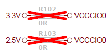
Figure 37: example of VCCIO0 assembly not dependent on 2.5V power rail. The other way is also possible.
| Others options of VCCIO0 power supply are not supported and can damage the FPGA! |
|---|
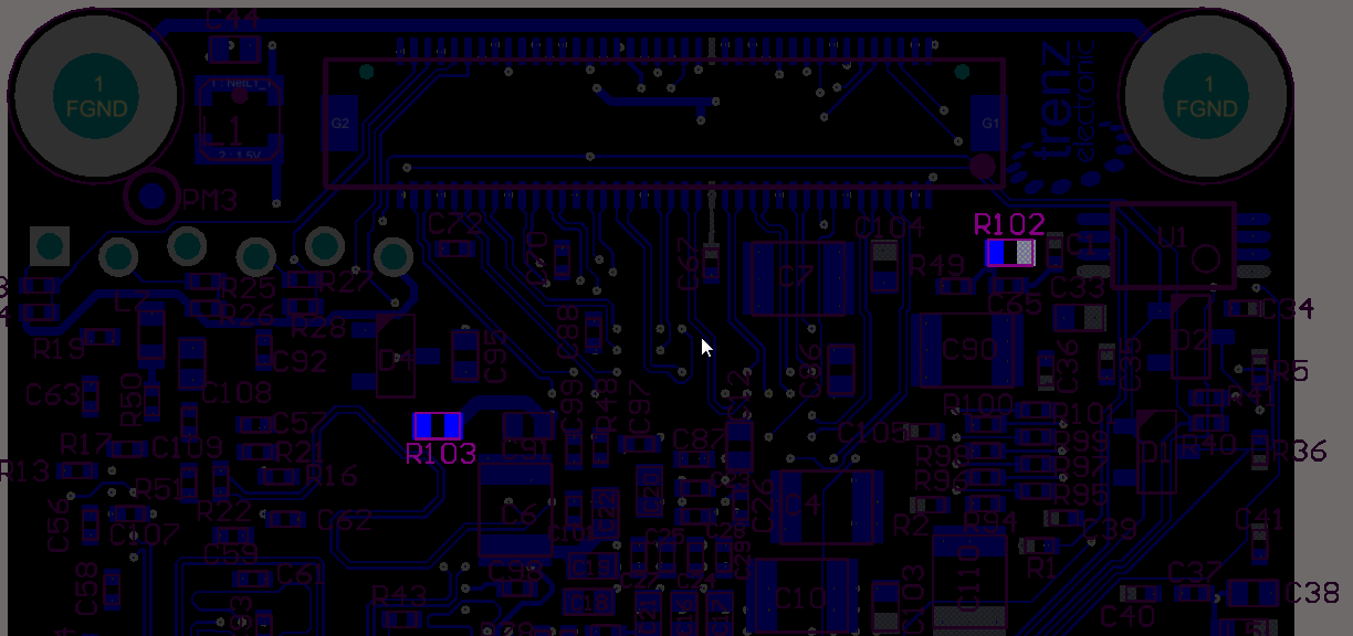
See Figure 4 to locate R102 and R103 on PCB.
Dip Switch S1B = FX2 PON
...
- Dynamic full power operation (PS_EN = 1): when the EZ-USB FX2LP USB FX2 microcontroller sets signal PS_EN = FX2_PS_EN = high, power rails 1.2 V, 1.5 V and 2.5 V are enabled.
This setting can be useful for . - Dynamic low power operation (PS_EN = 0): when the EZ-USB FX2LP USB FX2 microcontroller resets signal PS_EN = FX2_PS_EN = low, the following components are switched off:
- FPGA core logic (1.2V2 V)
- DDR SDRAM (2.5V5 V)
- FPGA bank 3 1 (2.5V5 V)VREF
- VREF1 (20.5V75 V)
- VCCCIO0 (2.5V5 V) FPGA bank 0 (if R131R102+R132R103- assembly)
Dip Switch S1B = PON
...
Overview
Content Tools