...
| Page properties |
|---|
|
Note for Download Link of the Scroll ignore macro: |
| Scroll pdf ignore |
|---|
Table of Contents |
...
The Trenz Electronic TE0716 is a commercial-grade* SoM (System on Module) based on Xilinx Zynq-7000 SoC XC7Z020*, with 1GB of DDR3L-1600 SDRAM*, 32MB of SPI flash memory, 10x 12-Bit Low Power SAR ADCs, 512Kb Serial EEPROM, Gigabit Ethernet PHY transceiver, a an USB PHY transceiver, a single chip USB 2.0 to UART/JTAG Interface (Xilinx License included), and powerful switching-mode power supplies for all on-board voltages. A large number of configurable I/Os are provided via rugged high-speed board-to-board connectors.
Refer to http://trenz.org/te0716-info for the current online version of this manual and other available documentation.
Notes: * standard values but depends on assembly version. Additional assembly options are available for cost or performance optimization upon request.
...
| Page properties |
|---|
|
Note:
'description: Important components and connector or other Features of the module
→ please sort and indicate assembly options Key Features' must be split into 6 main groups for modules and mainboards: - SoC/FPGA
- Package: SFVC784
- Device: ZU2...ZU5*
- Engine: CG, EG, EV*
- Speed: -1LI, -2LE,*, **
- Temperature: I, E,*, **
- RAM/Storage
- Low Power DDR4 on PS
- Data width: 32bit
- Size: def. 2GB*
- Speed:***
- eMMC
- Data width: 8Bit
- size: def. 8GB *
- QSPI boot Flash in dual parallel mode (size depends on assembly version)
- Data width: 8bit
- size: def. 128MB *
- HyperRAM/Flash (optional, default not assembled)
- MAC address serial EEPROM with EUI-48™ node identity (Microchip 24AA025E48)
- On Board
- Lattice LCMXO2
- PLL SI5338
- Gigabit Ethernet transceiver PHY (Marvell Alaska 88E1512)
- Hi-speed USB2 ULPI transceiver with full OTG support (Microchip USB3320C)
- Interface
- 132 x HP PL I/Os (3 banks)
- ETH
- USB
- 4 GTR (for USB3, Sata, PCIe, DP)
- MIO for UART
- MIO for SD
- MIO for PJTAG
- JTAG
- Ctrl
- Power
- 3.3V-5V Main Input
- 3.3V Controller Input
- Variable Bank IO Power Input
- Dimension
- Notes
- * depends on assembly version
- ** also non low power assembly options possible
- *** depends on used U+ Zynq and DDR4 combination
Key Features' must be split into 6 main groups for carrier: - Modules
- TE0808, TE807, TE0803,...
- RAM/Storage
- On Board
- Interface
- E.g. ETH, USB, B2B, Display port
- Power
- E.g. Input supply voltage
- Dimension
|
- SoC/FPGA
- Package: SFVC784 CLG484
- Device: Xilinx Z-7020
- Speed: -1 *
- Temperature: C grade *.
- Xilinx XC7Z020 SoC:
- Processing system (PS):
- ARM® CortexTM-A9 MPCoreTM with CoreSightTM.
- L1 Cache: 32KB Instruction, 32KB Data per processor.
- L2 Cache: 512KB.
- Programmable logic (PL):
- Artix-7 FPGA Equivalent.
- Logic cells: 85K.
- Look-Up Tables: 53200.
- Block RAM: 4.9 Mb.
- DSP slices: 220.
- Peak DSP performance: 276 GMACs.
- 2x 12 bit, 1 MSPS ADCs with up to 17 Differential Inputs.
- 120 x PL HR I/O (48 differential pairs and 24 single-ended).
- 2x PS MIOs (shared with UART TX/RX ZYNQ-FTDI).
- 1GByte DDR3L SDRAM memory (2 x [256Mbit x 16]), 32-bit wide data bus.
- 32MByte Quad SPI Flash memory.
- MAC address serial EEPROM with EUI-48TM node identity (24AA025E48).
- 512Kb Serial EEPROM memory (CAT24C512).
- 10x 12-Bit Low Power SAR ADCs up to 2 MSPS (NCD98011).
- Gigabit Ethernet transceiver PHY (Marvell 88E1512).
- Highly integrated full-featured hi-speed USB 2.0 ULPI transceiver (Microchip USB3320C-EZK).
- RAM/Storage
- Low Power DDR3 SDRAM on PS
- Data width: 32bit
- Size: def. 1GB *
- Speed: 1600 Mbps **
- QSPI boot Flash
- Data width: 4bit
- size: 32MB *
- MAC address serial EEPROM with EUI-48™ node identity (Microchip 24AA025E48).
- 512Kb user MAC address serial EEPROM.
- On Board
- 10x 12-Bit Low Power SAR ADCs up to 2 MSPS (NCD98011).
- Low Power Oscillators.
- Gigabit Ethernet PHY transceiver (Marvell Alaska 88E1512).
- High-Speed USB 2.0 ULPI transceiver with full OTG support (Microchip USB3320C).
- Single chip High-Speed USB 2.0 to UART/JTAG Interface (Xilinx License included) (FTDI FT2232H).
- 2x User RGB LEDs (Green), LED FPGA "Done" (Green).
- 2x Tactile Switches (User), 1 x Tactile Switche (Reset).
- Interface
- 120x HR PL I/Os (3 banks).
- 2x PS MIOs (shared with UART TX/RX ZYNQ-FTDI).
- 1 Gbps RGMII Ethernet interface.
- High Speed USB 2.0 ULPI with full OTG support.
- High Speed USB 2.0 to UART/JTAG interface
Single chip USB Interface 2.0 High Speed 480Mbs to UART / JTAG(Xilinx License included) (FTDI FT2232H-56Q)- , including microUSB-B connector.
- 2xUser RGB LEDs (Green), LED FPGA DONE (Green).
- 2 x Tactile Switches (User), 1 x Tactile Switche (Reset).
- PowerCard Connector microSD™.
- On-board high-efficiency DC-DC converters for all voltages used.
- DimensionBoard Size: .
Block Diagram
- Notes
- * depends on assembly version
- ** depends on used Zynq and DDR3 combination
Block Diagram
| Page properties |
|---|
| Page properties |
|---|
|
add drawIO object here.
|
...
| Scroll Title |
|---|
| anchor | Figure_OV_BD |
|---|
| title | TExxxx TE0716-01 block diagram |
|---|
|
| Scroll Ignore |
|---|
| draw.io Diagram |
|---|
| border | false |
|---|
| |
|---|
| diagramName | DB-TE0716-01 |
|---|
| simpleViewer | false |
|---|
| width | |
|---|
| links | auto |
|---|
| tbstyle | hidden |
|---|
| diagramDisplayName | |
|---|
| lbox | true |
|---|
| diagramWidth | 641 |
|---|
| revision | 919 |
|---|
|
|
| Scroll Only |
|---|
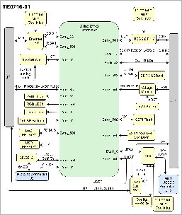 Image Removed Image Removed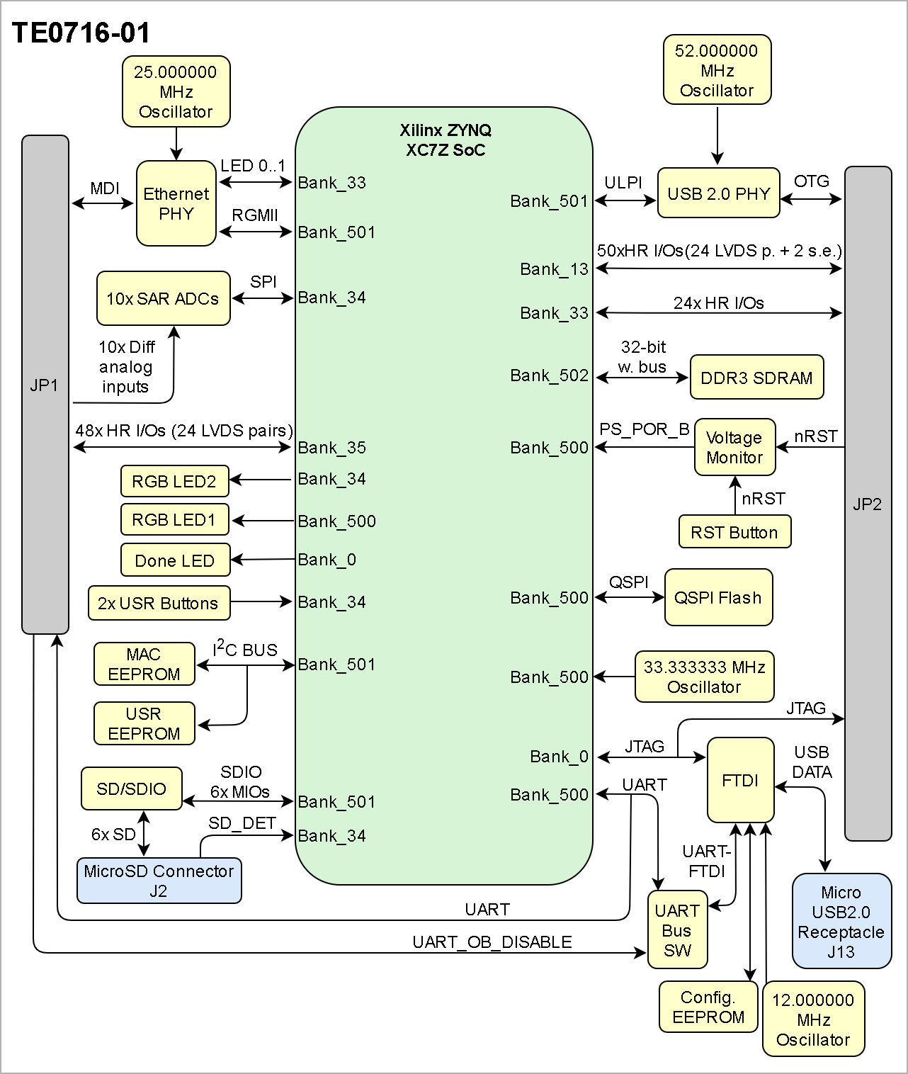 Image Added Image Added
|
|
Main Components
...
| Scroll Title |
|---|
| anchor | Figure_OV_MC |
|---|
| title | TExxxx TE0716-01 main components |
|---|
|
| Scroll Ignore |
|---|
| draw.io Diagram |
|---|
| border | false |
|---|
| |
|---|
| diagramName | MC-TE0716-01 |
|---|
| simpleViewer | false |
|---|
| width | |
|---|
| links | auto |
|---|
| tbstyle | hidden |
|---|
| diagramDisplayName | |
|---|
| lbox | true |
|---|
| diagramWidth | 641 |
|---|
| revision | 1418 |
|---|
|
|
| Scroll Only |
|---|
 Image Modified Image Modified
|
|
- Xilinx Zynq XC7Z SoC, U5 (Top)
- 4Gbit DDR3/L SDRAM, U13 (Top)
- 4Gbit DDR3/L SDRAM, U12 (Top)
- 32MByte Quad SPI Flash memory, U7 (Top)
- 2Kbit MAC address serial EEPROM with EUI-48TM node identity, U24
Initial Delivery State
| Page properties |
|---|
|
Notes : Only components like EEPROM, QSPI flash can be initialized by default at manufacture. If there is no components which might have initial data ( possible on carrier) you must keep the table empty |
...
| anchor | Table_OV_IDS |
|---|
| title | Initial delivery state of programmable devices on the module |
|---|
...
Storage device name
...
Content
...
Notes
...
Quad SPI Flash
...
-
...
-
...
- (Top)
- 512Kb Serial EEPROM memory, U21 (Top)
- 10x 12-Bit Low Power SAR ADCs, U1..U4, U10, U11, U15..U17, U19 (Top)
- High-speed USB 2.0 ULPI transceiver, U18 (Top)
- Single chip USB Interface 2.0 to UART / JTAG, U39 (Top)
- MicroUSB-B connector, J13 (Top)
- Low-power oscillator @ 12.000000MHz (OSCI-FTDI), U41 (Top)
- Low-power oscillator @ 25.000000MHz (ETH-CLK), U9 (Top)
- LED FPGA "Done" (Green) D3 (Top)
- User RGB LED 1 D4 (Top)
- User RGB LED 2 D5 (Top)
- Tactile Switch (User), S1 (Top)
- Tactile Switch (User), S2 (Top)
- Tactile Switch (Reset), S3 (Top)
- 5A Synchronous Buck DC-DC Converter (1V), U37 (Top)
- 2A Synchronous Buck DC-DC Converter (3.3V), U46 (Top)
- 2A Synchronous Buck DC-DC Converter (1.8V), U45 (Top)
- 2A Synchronous Buck DC-DC Converter (1.5V), U43 (Top)
- 250mA Ultra-Low Noise LDO Regulator (3.3V_ADC Digital I/O supply), U23 (Top)
- 250mA Ultra-Low Noise LDO Regulator (ADC_VAA Analog supply/reference, 3.3V), U38 (Top)
- Gigabit Ethernet PHY transceiver, U8 (Bottom)
- Low-power oscillator @ 33.333333MHz (PS-CLK), U6 (Bottom)
- 3A Sink/Source DDR Termination Regulator (VTT/VTTREF, 0.75V), U47 (Bottom)
- Card Connector microSD™, J2 (Bottom)
- 2x60 positions high speed/density plug connector, JP1 (Bottom)
- 2x60 positions high speed/density plug connector, JP2 (Bottom)
Initial Delivery State
| Page properties |
|---|
|
Notes : Only components like EEPROM, QSPI flash can be initialized by default at manufacture. If there is no components which might have initial data ( possible on carrier) you must keep the table empty |
| Scroll Title |
|---|
| anchor | Table_OV_IDS |
|---|
| title | Initial delivery state of programmable devices on the module |
|---|
|
|
Configuration Signals
| Page properties |
|---|
|
- Overview of Boot Mode, Reset, Enables.
|
Boot process.
The TE0716 supports QSPI and SD Card boot modes, which is controlled by the insertion of the SD card before powering on.
| Scroll Title |
|---|
| anchor | Table_OV_BP |
|---|
| title | Boot process. |
|---|
|
| Scroll Table Layout |
|---|
| orientation | portrait |
|---|
| sortDirection | ASC |
|---|
| repeatTableHeaders | default |
|---|
| style | |
|---|
| widths | |
|---|
| sortByColumn | 1 |
|---|
| sortEnabled | false |
|---|
| cellHighlighting | true |
|---|
|
Storage device name | IC Designator | Content |
|---|
SD Card State | Boot ModeSD card inserted | SD Card (J2) | - | | SD card not present | QSPI (U7) | - | |
Reset process.
The nRST signal active low reset input, forces PS_POR_B to apply a master reset of the entire Zynq. This reset could be manually done by pressing a switch. This signal could be also reached by a B2B large connector.
This nRST signal (active low) is also held until all FPGA power supplies set their Power Good signals.
Furthermore, if the FPGA core voltage drops under 0.84V or the 3.3V power supply drops to 2.94V or less, this nRST signal is also activated by the Voltage Monitor.
See more about the Power-on Reset (PS_POR_B) signal in the “Zynq-7000 SoC Technical Reference Manual” (“UG585”).
Quad SPI Flash | U7 | Empty | - | | 512Kb Serial EEPROM | U21 | Empty | - | | 2Kb 24AA025E48 EEPROM | U24 | Pre-programmed globally unique, 48-bit node address (MAC). | - | | 4Kb M93C66-R EEPROM | U40 | Xilinx JTAG Programmer License | For FTDI IC only (U39). |
|
Configuration Signals
| Page properties |
|---|
|
- Overview of Boot Mode, Reset, Enables.
|
Boot process.
The TE0716 supports QSPI and SD Card boot modes, which is controlled by the insertion of the SD card before powering on.
| Scroll Title |
|---|
| anchor | Table_OV_BP |
|---|
| title | Boot process. |
|---|
|
| Scroll Table Layout |
|---|
| orientation | portrait |
|---|
| sortDirection | ASC |
|---|
|
|
| Scroll Title |
|---|
| anchor | Table_OV_RST |
|---|
| title | Reset process. |
|---|
|
| Scroll Table Layout |
|---|
| orientation | portrait |
|---|
| sortDirection | ASC |
|---|
| repeatTableHeaders | default |
|---|
| style | |
|---|
| widths | |
|---|
| sortByColumn | 1 |
|---|
| sortEnabled | false |
|---|
| cellHighlighting | true |
|---|
|
|
Signal | B2B | I/O | Note |
|---|
nRST | JP2-4 | - | - |
| nRST | - | S3 | - |
Signals, Interfaces and Pins
| Page properties |
|---|
|
Notes : - For carrier or stand-alone boards use subsection for every connector type (add designator on description, not on the subsection title), for example:
- For modules which needs carrier use only classes and refer to B2B connector if more than one is used, for example
|
Board to Board (B2B) I/Os
SD Card State | Boot Mode | Notes |
|---|
SD card inserted | SD Card (J2) | - | | SD card not present | QSPI (U7) | - |
|
Reset process.
The nRST signal active low reset input, forces PS_POR_B to apply a master reset of the entire Zynq. This reset could be manually done by pressing a switch. This signal could be also reached by a B2B large connector.
This nRST signal (active low) is also held until all FPGA power supplies set their Power Good signals.
Furthermore, if the FPGA core voltage drops under 0.84V or the 3.3V power supply drops to 2.94V or less, this nRST signal is also activated by the Voltage Monitor.
See more about the Power-on Reset (PS_POR_B) signal in the “Zynq-7000 SoC Technical Reference Manual” (“UG585”).Zynq SoC's I/O banks signals connected to the B2B connectors:
| Scroll Title |
|---|
| anchor | Table_SIPOV_B2BRST |
|---|
| title | General PL I/O to B2B connectors informationReset process. |
|---|
|
| Scroll Table Layout |
|---|
| orientation | portrait |
|---|
| sortDirection | ASC |
|---|
| repeatTableHeaders | default |
|---|
| style | |
|---|
| widths | |
|---|
| sortByColumn | 1 |
|---|
| sortEnabled | false |
|---|
| cellHighlighting | true |
|---|
|
FPGA Bank Connector Signal CountVoltage Level| Notes | MIO 500 | JP1 | 2 | 3.3VHR 35JP1 | 48 | 3.3V | - | | HR 13 | JP2 | 50 | 3.3V | - | | HR 33 | JP2 | 22 | 3.3V | - | |
...
Signals, Interfaces and Pins
| Page properties |
|---|
|
Notes : - For carrier or stand-alone boards use subsection for every connector type (add designator on description, not on the subsection title), for example:
- For modules which needs carrier use only classes and refer to B2B connector if more than one is used, for example
|
Board to Board (B2B)
FPGA IOs
Zynq SoC's I/O banks signals connected to the B2B connectors:JTAG access to the TExxxx SoM through B2B connector JMX.
| Scroll Title |
|---|
| anchor | Table_SIP_JTGB2B |
|---|
| title | JTAG pins connectionGeneral PS-PL I/O to B2B connectors information |
|---|
|
| Scroll Table Layout |
|---|
| orientation | portrait |
|---|
| sortDirection | ASC |
|---|
| repeatTableHeaders | default |
|---|
| style | |
|---|
| widths | |
|---|
| sortByColumn | 1 |
|---|
| sortEnabled | false |
|---|
| cellHighlighting | true |
|---|
|
JTAG Signal| TMS | JP2-7 | | TDI | JP2-11 | | TDO | JP2-10 | | TCK | JP2-8 | |
MIO Pins
| I/O Signal Count | Voltage Level | Notes |
|---|
| MIO 500 | JP1 | 2 | 3.3V | - | | HR 35 | JP1 | 48 | 3.3V | - | | HR 13 | JP2 | 50 | 3.3V | - | | HR 33 | JP2 | 22 | 3.3V | - |
|
JTAG Interface
JTAG access to the TE0716 SoM through B2B connector JP2. The TE0716 is also provided with a FTDI USB-to-JTAG adapter connected to the MicroUSB connector J13, but ONLY ONE connection for JTAG should be used at the time!.
| scroll |
|---|
| Page properties |
|---|
|
you must fill the table below with group of MIOs which are connected to a specific components or peripherals, you do not have to specify pins in B2B, Just mention which B2B is connected to MIOs. The rest is clear in the Schematic.
Example:
| MIO Pin | Connected to | B2B | Notes |
|---|
| MIO12...14 | SPI_CS , SPI_DQ0... SPI_DQ3 SPI_SCK | J2 | QSPI |
| scroll-title |
|---|
| anchor | Table_SIP_MIOsJTG |
|---|
| title | MIOs JTAG pins connection |
|---|
|
| Scroll Table Layout |
|---|
| orientation | portrait |
|---|
| sortDirection | ASC |
|---|
| repeatTableHeaders | default |
|---|
| style | |
|---|
| widths | |
|---|
| sortByColumn | 1 |
|---|
| sortEnabled | false |
|---|
| cellHighlighting | true |
|---|
|
| MIO Pin | Connected to | B2B| 15 | UART_TX_ZYNQ | JP1-70 | Also Connected to U36-2. To use this signal from B2B connector, "UART_OB_DISABLE" (JP1-11) must be "High". | | 14 | UART_RX_ZYNQ | JP1-71 | Also Connected to U36-3. To use this signal from B2B connector, "UART_OB_DISABLE" (JP1-11) must be "High". | |
Test Points
...
you must fill the table below with group of Test Point which are indicated as TP in a schematic. If there is no Test Point remarked in the schematic, delet the Test Point section.
Example:
| TMS | JP2-7 | 3.3V Voltage level. Also Connected to U39 (FTDI) | | TDI | JP2-11 | 3.3V Voltage level. Also Connected to U39 (FTDI) | | TDO | JP2-10 | 3.3V Voltage level. Also Connected to U39 (FTDI) | | TCK | JP2-8 | 3.3V Voltage level. Also Connected to U39 (FTDI) | | VREF_JTAG | JP2-5 | Module Vout |
|
UART Interface
...
The TE0716 provides UART access to the TE0716 SoM through B2B connector JP1. The TE0716 is also equipped with a FTDI USB-to-UART adapter connected to the MicroUSB connector J13, but ONLY ONE connection for UART should be used at the time! (please read "Notes" in the following table). The UART interface is connected to the Zynq UART PS (UART 0).
| Scroll Title |
|---|
| anchor | Table_SIP_TPsUART |
|---|
| title | Test Points InformationUART pins connection |
|---|
|
| Scroll Table Layout |
|---|
| orientation | portrait |
|---|
| sortDirection | ASC |
|---|
| repeatTableHeaders | default |
|---|
| style | |
|---|
| widths | |
|---|
| sortByColumn | 1 |
|---|
| sortEnabled | false |
|---|
| cellHighlighting | true |
|---|
|
| Test Point | Connected toTP1 | +1.0V | - | TP2 | ADC_VAA | - | TP3 | +1.5V | - | TP4 | +1.8V | - | TP5 | VTT | - | TP6 | VTTREF | - | TP7 | +5.0V | - | TP8 | +3.3V | - | TP9 | +5.0V_VAA | - | TP10 | +3.3V_ADC | - | TP11 | GND | - | TP12 | GND | - | TP13 | SPI-DQ3/M0 | TP14 | GND | |
On-board Peripherals
| Page properties |
|---|
|
Notes : - add subsection for every component which is important for design, for example:
- Two 100 Mbit Ethernet Transciever PHY
- USB PHY
- Programmable Clock Generator
- Oscillators
- eMMCs
- RTC
- FTDI
- ...
- DIP-Switches
- Buttons
- LEDs
|
...
Notes :
...
| UART_TX_ZYNQ | JP1-70 | 3.3V Voltage level. Also Connected to FTDI through U36. To use this signal from B2B connector, "UART_OB_DISABLE" (JP1-11) must be "High". | | UART_RX_ZYNQ | JP1-71 | 3.3V Voltage level. Also Connected to FTDI through U36. To use this signal from B2B connector, "UART_OB_DISABLE" (JP1-11) must be "High". |
|
USB Interface
The TE0716 provides USB access to the TE0716 SoM through B2B connector JP2. The USB interface is connected later to the Zynq UART PS (USB 0), by using a USB PHY.
| Scroll Title |
|---|
| anchor | Table_SIP_USB |
|---|
| title | USB pins connection |
|---|
|
| Scroll Table Layout |
|---|
| orientation | portrait |
|---|
| sortDirection | ASC |
|---|
| repeatTableHeaders | default |
|---|
| style | |
|---|
| widths | |
|---|
| sortByColumn | 1 |
|---|
| sortEnabled | false |
|---|
| cellHighlighting | true |
|---|
|
USB Signal | B2B Connector | Notes |
|---|
| USB_OTG_D_ P | JP2-64 | 3.3V Voltage level. | | USB_OTG_D_ N | JP2-65 | 3.3V Voltage level. | | USB_OTG_ID | JP2-66 | 3.3V Voltage level. | | USB_VBUS_E N | JP2-67 | 3.3V Voltage level. | | USB_VBUS | JP2-68 | Max. voltage: 5.5V |
|
ETH Interface
The TE0716 provides ETH access to the TE0716 SoM through B2B connector JP1. The ETH interface is connected later to the Zynq Ethernet PS (Ethernet 0), by using a ETH PHY.
| Scroll Title |
|---|
| anchor | Table_OBPSIP_ETH |
|---|
| title | On board peripheralsETH pins connection |
|---|
|
| Scroll Table Layout |
|---|
| orientation | portrait |
|---|
| sortDirection | ASC |
|---|
| repeatTableHeaders | default |
|---|
| style | |
|---|
| widths | |
|---|
| sortByColumn | 1 |
|---|
| sortEnabled | false |
|---|
| cellHighlighting | true |
|---|
|
|
Quad SPI Flash Memory
| Page properties |
|---|
|
Notes : Minimum and Maximum density of quad SPI flash must be mentioned for other assembly options. |
On-board 32MByte QSPI flash memory S25FL256S (U7) could be used to store the initial FPGA configuration file. After configuration completes, the remaining free memory can be used for application data storage. All four SPI data lines are connected to the FPGA allowing x1, x2 or x4 data bus widths. Maximum data rate depends on the selected bus width and clock frequency used.
...
PHY_MDI0_P PHY_MDI0_ N | JP1-5 JP1-4 | 3.3V Voltage level. | PHY_MDI1_P PHY_MDI1_ N | JP1-7 JP1-8 | 3.3V Voltage level. | PHY_MDI2_P PHY_MDI2_ N | JP1-68 JP1-67 | 3.3V Voltage level. | PHY_MDI3_P PHY_MDI3_ N | JP1-65 JP1-64 | 3.3V Voltage level. |
|
ADC Interface
The analog inputs of the ADCs are connected to B2B connector JP1
...
.
| Scroll Title |
|---|
| anchor | Table_OBPSIP_SPIADCs |
|---|
| title | Quad SPI interface MIOs and ADCs pins connection |
|---|
|
| Scroll Table Layout |
|---|
| orientation | portrait |
|---|
| sortDirection | ASC |
|---|
| repeatTableHeaders | default |
|---|
| style | |
|---|
| widths | |
|---|
| sortByColumn | 1 |
|---|
| sortEnabled | false |
|---|
| cellHighlighting | true |
|---|
|
|
| MIO Pin | Schematic | U7 Pin | Notes |
|---|
...
The TE0716 module has 10x 12-Bit Low Power SAR Analog-to-Digital Converter, fully differential input, signed output, with SPI−compatible interface (NCD98011), which are connected to the FPGA PL BANK34.
- Part number: NCD98011XMXTAG
- Analog supply and ADC reference voltage: 3.3V (1.65V – 3.6V).
- Digital I/O supply voltage: 3.3V (1.65V – 3.6V).
- Differential analog inputs: 1 per ADC.
- Sampling rate: 2 MSPS max.
- SNR: 70dB @1KHz fIN.
- THD: -80dB @1KHz fIN.
- Junction Temperature: Range -40°C to +125°C.
ADC Signal | B2B Connector | Notes |
|---|
ADC0_P
ADC0_N | JP1-106..107 | SAR ADC, U1.
3.3V Max. Voltage on any pin. | ADC1_P
ADC1_N | JP1-46..47 | SAR ADC, U3.
3.3V Max. Voltage on any pin. | ADC2_P
ADC2_N | JP1-109..110 | SAR ADC, U10.
3.3V Max. Voltage on any pin. | ADC3_P
ADC3_N | JP1-49..50 | SAR ADC, U15.
3.3V Max. Voltage on any pin. | ADC4_P
ADC4_N | JP1-112..113 | SAR ADC, U17.
3.3V Max. Voltage on any pin. | ADC5_P
ADC5_N | JP1-52..53 | SAR ADC, U2.
3.3V Max. Voltage on any pin. | ADC6_P
ADC6_N | JP1-115..116 | SAR ADC, U4.
3.3V Max. Voltage on any pin. | ADC7_P
ADC7_N | JP1-55..56 | SAR ADC, U11.
3.3V Max. Voltage on any pin. | ADC8_P
ADC8_N | JP1-118..119 | SAR ADC, U16.
3.3V Max. Voltage on any pin. | ADC9_P
ADC9_N | JP1-58..59 | SAR ADC, U19.
3.3V Max. Voltage on any pin. |
|
PWM Interface
The PWM signals are connected to B2B connector JP2. All this digital signals are connected to PL Bank 33 (except for PWM_6_H and PWM_6_L which are connected to PL Bank 13). These signals could be also used as normal single ended I/Os.
| Scroll Title |
|---|
| anchor | Table_SIP_PWMs |
|---|
| title | PWMs pins connection |
|---|
|
|
| Scroll Title |
|---|
| anchor | Table_OBP_RTC |
|---|
| title | I2C interface MIOs and pins |
|---|
|
| Scroll Table Layout |
|---|
| orientation | portrait |
|---|
| sortDirection | ASC |
|---|
| repeatTableHeaders | default |
|---|
style | widths | | sortByColumn | 1 |
|---|
| sortEnabled | false |
|---|
| cellHighlighting | true |
|---|
| MIO Pin | Schematic | U? Pin | Notes |
|---|
| Scroll Title |
|---|
| anchor | Table_OBP_I2C_RTC |
|---|
| title | I2C Address for RTC |
|---|
|
| Scroll Table Layout |
|---|
| orientation | portrait |
|---|
| sortDirection | ASC |
|---|
| repeatTableHeaders | default |
|---|
| style | |
|---|
| widths | |
|---|
| sortByColumn | 1 |
|---|
| sortEnabled | false |
|---|
| cellHighlighting | true |
|---|
|
| MIO Pin | I2C Address | Designator |
...
MAC-Address EEPROM
A 2Kbit 24AA025E48 serial EEPROM I2C memory (U24), connected to the BANK501 PSMIOs, contains a globally unique 48-bit node address, which is compatible with EUI-48TM specification. The device is organized as two blocks of 128 x 8-bit memory. One of the blocks, the upper half of the array (80h-FFh), stores the 48-bit node address and is permanently write-protected, while the other block is available for application use.
- Part number: 24AA025E48T-I/OT
- Supply voltage: 1.8V (1.7V - 5.5V).
- FCLK: 100KHz (@VCC=1.8V)
- Temperature: Industrial Range -40°C to +85°C.
...
| anchor | Table_OBP_EEP |
|---|
| title | I2C EEPROM interface MIOs and pins |
|---|
...
General Purpose EEPROM
- The TE0716 module has also a 512Kb Serial EEPROM I2C memory (U21).
- Part number: CAT24C512WI-GT3
- Supply voltage: 1.8V (1.8V - 5.5V).
- FCLK: 100KHz/400KHz/1MHz
- Temperature: Industrial Range -40°C to +85°C.
...
| anchor | Table_OBP_I2C_EEPROM |
|---|
| title | I2C address for EEPROM |
|---|
...
0xA6 (write)
0xA7 (read)
0x53 (7bit)
...
| PWM_0_H | JP2-103 | 3.3V Max. Voltage on any pin. | | PWM_0_L | JP2-104 | 3.3V Max. Voltage on any pin. | | PWM_1_H | JP243 | 3.3V Max. Voltage on any pin. | | PWM_1_L | JP2-44 | 3.3V Max. Voltage on any pin. | | PWM_10_H | JP2-118 | 3.3V Max. Voltage on any pin. | | PWM_10_L | JP2-119 | 3.3V Max. Voltage on any pin. | | PWM_11_H | JP2-58 | 3.3V Max. Voltage on any pin. | | PWM_11_L | JP2-59 | 3.3V Max. Voltage on any pin. | | PWM_2_H | JP2-106 | 3.3V Max. Voltage on any pin. | | PWM_2_L | JP2-107 | 3.3V Max. Voltage on any pin. | | PWM_3_H | JP2-46 | 3.3V Max. Voltage on any pin. | | PWM_3_L | JP2-47 | 3.3V Max. Voltage on any pin. | | PWM_4_H | JP2-109 | 3.3V Max. Voltage on any pin. | | PWM_4_L | JP2-110 | 3.3V Max. Voltage on any pin. | | PWM_5_H | JP2-49 | 3.3V Max. Voltage on any pin. | | PWM_5_L | JP2-50 | 3.3V Max. Voltage on any pin. | | PWM_6_H | JP2-112 | 3.3V Max. Voltage on any pin. | | PWM_6_L | JP2-113 | 3.3V Max. Voltage on any pin. | | PWM_7_H | JP2-52 | 3.3V Max. Voltage on any pin. | | PWM_7_L | JP2-53 | 3.3V Max. Voltage on any pin. | | PWM_8_H | JP2-115 | 3.3V Max. Voltage on any pin. | | PWM_8_L | JP2-116 | 3.3V Max. Voltage on any pin. | | PWM_9_H | JP2-55 | 3.3V Max. Voltage on any pin. | | PWM_9_L | JP2-56 | 3.3V Max. Voltage on any pin. |
|
Micro USB -JTAG/UART
A microUSB-B connector (J13) is connected to the FTDI. It provides the ability to communicate to the PL FPGA via JTAG, as well as to the PS UART (UART 0).
Caution: because the TE0716 also provides UART and JTAG access to the FPGA through B2B connectors JP1 and JP2 respectively, ONLY ONE connection for UART, and ONLY ONE connection for JTAG, should be used at the time! (please read "UART Interface" and "JTAG Interface" above in the "Board to Board (B2B)" Section).
Micro SD Socket
A microSD™ card connector (J2) is connected via U35 (SD/SDIO Multiplexer - Level Translator) to Zynq PS (Bank501/SDIO 0). It is a Push-On/Push-Off socket type, and work with a voltage level of 3.3V.
MIO Pins
| Page properties |
|---|
|
you must fill the table below with group of MIOs which are connected to a specific components or peripherals, you do not have to specify pins in B2B, Just mention which B2B is connected to MIOs. The rest is clear in the Schematic. Example: | MIO Pin | Connected to | B2B | Notes |
|---|
| MIO12...14 | SPI_CS , SPI_DQ0... SPI_DQ3 SPI_SCK | J2 | QSPI |
|
PS MIO banks 500/501 signal connections to interface.
...
0xA0 (write)
0xA1 (read)
0x50 (7bit)
...
LEDs
...
| anchor | Table_OBP_LED |
|---|
| title | On-board LEDs |
|---|
...
DDR3 SDRAM
| Page properties |
|---|
|
Notes : Minimum and Maximum density of DDR3 SDRAM must be mentioned for other assembly options. (pay attention to supported address length for DDR3) |
The TE0716 module has two 500MByte DDR3L SDRAM chips (U12 & U13) arranged into 32-bit wide memory bus providing total on-board memory size of 1GByte.
- Part number: IS43TR16256BL-125KBLI
- Configuration: 256Mx16.
- Supply voltage: 1.35V (1.5V tolerant).
- Speed: 1.25ns @ CL11 (DDR3-1600)
- Temperature: Industrial Range -40°C to +95°C Tcase.
Ethernet
...
| anchor | Table_OBP_ETH |
|---|
| title | Ethernet PHY to Zynq SoC connections |
|---|
...
| Scroll Title |
|---|
| anchor | Table_OBPSIP_CANMIOs |
|---|
| title | CAN Tranciever interface MIOs pins |
|---|
|
| Scroll Table Layout |
|---|
| orientation | portrait |
|---|
| sortDirection | ASC |
|---|
| repeatTableHeaders | default |
|---|
| style | |
|---|
| widths | |
|---|
| sortByColumn | 1 |
|---|
| sortEnabled | false |
|---|
| cellHighlighting | true |
|---|
|
Bank| Schematic | U?? PinD-Tx | Driver Input | R-Rx | Reciever Output | |
...
| anchor | Table_OBP_CLK |
|---|
| title | Osillators |
|---|
...
Programmable Clock Generator
There is a programmable clock generator on-board (U??) provided in order to generate variable clocks for the module. Programming can be done using I2C via PIN header J??. The I2C Address is 0x??.
...
| anchor | Table_OBP_PCLK |
|---|
| title | Programmable Clock Generator Inputs and Outputs |
|---|
| Scroll Table Layout |
|---|
| orientation | portrait |
|---|
| sortDirection | ASC |
|---|
| repeatTableHeaders | default |
|---|
| sortByColumn | 1 |
|---|
| sortEnabled | false |
|---|
| cellHighlighting | true |
|---|
|
...
IN0
...
XAXB
...
Power and Power-On Sequence
...
In 'Power and Power-on Sequence' section there are three important digrams which must be drawn:
- Power on-sequence
- Power distribution
- Voltage monitoring circuit
| Note |
|---|
For more information regarding how to draw diagram, Please refer to "Diagram Drawing Guidline" . |
|
|---|
| 1..6 | SPI-CS , SPI-DQ0... SPI-DQ3 SPI-SCK | - | QSPI Flash, U7 | | 11..13 | LED1_R..G..B | - | LED D4 | | 14, 15 | UART_RX_ZYNQ, UART_TX_ZYNQ | JP1 | 3.3V Voltage level. Also Connected to U36-2. To use this signal from B2B connector, "UART_OB_DISABLE" (JP1-11) must be "High". | | 16..27 | ETH-TXCK, ETH-TXD0..ETH-TXD3, ETH-TXCTL, ETH-RXCK, ETH-RXD0..ETH-RXD3, ETH-RXCTL | - | Gigabit ETH Transceiver, U8 | | 28..39 | OTG-DATA0..OTG-DATA7, OTG-DIR, OTG-STP, OTG-NXT, OTG-CLK | - | USB 2.0 ULPI transceiver, U18 | | 40..45 | PS_SD_CLK, PS_SD_CMD, PS_SD_DAT0..PS_SD_DAT3 | J2 | 3.3V Voltage level. Connected to PS via U35 (SD/SDIO Multiplexer - Level Translator) | | 46, 47 | I2C_SCL, I2C_SDA | - | General Purpose EEPROM, U21
MAC EEPROM, U24 | | 51 | PHY-RST | - | Gigabit ETH Transceiver, U8
USB 2.0 ULPI transceiver, U18 | | 52, 53 | ETH-MDC, ETH-MDIO | - | Gigabit ETH Transceiver, U8 |
|
Test Points
| Page properties |
|---|
|
you must fill the table below with group of Test Point which are indicated as TP in a schematic. If there is no Test Point remarked in the schematic, delet the Test Point section. Example: | Test Point | Signal | B2B | Notes |
|---|
| 10 | PWR_PL_OK | J2-120 |
|
|
| Scroll Title |
|---|
| anchor | Table_SIP_TPs |
|---|
| title | Test Points Information |
|---|
|
| Scroll Table Layout |
|---|
| orientation | portrait |
|---|
| sortDirection | ASC |
|---|
| repeatTableHeaders | default |
|---|
| style | |
|---|
| widths | |
|---|
| sortByColumn | 1 |
|---|
| sortEnabled | false |
|---|
| cellHighlighting | true |
|---|
|
| Test Point | Signal | Connected to | Notes |
|---|
| TP1 | +1.0V | U37, DC-DC Converter
| PL-VCCINT | | TP2 | ADC_VAA | U38, LDO Regulator
| ADC_VAA Analog supply/reference, (3.3V) | | TP3 | +1.5V | U43, DC-DC Converter | - | | TP4 | +1.8V | U45, DC-DC Converter | - | | TP5 | VTT | U47, DDR Termination Regulator | (0.75V) | | TP6 | VTTREF | U47, DDR Termination Regulator | (0.75V) | | TP7 | +5.0V | JP1-(1,2,3)
JP2-(1,2,3) | Main Digital Power Input | | TP8 | +3.3V | U46, DC-DC Converter | - | | TP9 | +5.0V_VAA | JP1-(43,44) | Main Analog Low Power Input | | TP10 | +3.3V_ADC | U23, LDO Regulator | ADC's Digital I/O supply | | TP11 | GND | - | - | | TP12 | GND | - | - | | TP13 | SPI-DQ3/M0 | MIO_5 | Remove SD card and short with TP14 for JTAG only mode | | TP14 | GND | - | - |
|
On-board Peripherals
| Page properties |
|---|
|
Notes : - add subsection for every component which is important for design, for example:
- Two 100 Mbit Ethernet Transciever PHY
- USB PHY
- Programmable Clock Generator
- Oscillators
- eMMCs
- RTC
- FTDI
- ...
- DIP-Switches
- Buttons
- LEDs
|
| Page properties |
|---|
|
Notes : In the on-board peripheral table "chip/Interface" must be linked to the corresponding chapter or subsection |
| Scroll Title |
|---|
| anchor | Table_OBP |
|---|
| title | On board peripherals |
|---|
|
| Scroll Table Layout |
|---|
| orientation | portrait |
|---|
| sortDirection | ASC |
|---|
| repeatTableHeaders | default |
|---|
| style | |
|---|
| widths | |
|---|
| sortByColumn | 1 |
|---|
| sortEnabled | false |
|---|
| cellHighlighting | true |
|---|
|
| Chip/Interface | Designator | Notes |
|---|
| DDR3 SDRAM | U12, U13 | - | | Quad SPI Flash | U7 | - | | MAC EEPROM | U24 | - | | General Purpose EEPROM | U21 | - | | SAR ADCs | U1, U2, U3, U4, U10, U11, U15, U16, U17, U19 | - | | Clock Sources | U6, U9, U14, U41 | - | | Gigabit Ethernet PHY | U8 | - | | USB 2.0 ULPI transceiver | U18 | - | | FTDI USB 2.0 to UART/JTAG | U39 | - | | LEDs | D3, D4, D5 | - | | Switches | S1, S2, S3 | - |
|
DDR3 SDRAM
| Page properties |
|---|
|
Notes : Minimum and Maximum density of DDR3 SDRAM must be mentioned for other assembly options. (pay attention to supported address length for DDR3) |
The TE0716 module has two 500MByte DDR3L SDRAM chips (U12 & U13) fully connected to PS DDR BANK 502, and arranged into 32-bit wide memory bus providing total on-board memory size of 1GByte.
- Configuration: 256Mx16*
- Supply voltage: 1.35V (1.5V tolerant).
- Speed: 1.25ns @ CL11 (DDR3-1600)*
- Temperature: Industrial Range -40°C to +95°C Tcase.
Notes: * standard value but depends on assembly version.
Quad SPI Flash Memory
| Page properties |
|---|
|
Notes : Minimum and Maximum density of quad SPI flash must be mentioned for other assembly options. |
On-board 32MByte QSPI flash memory S25FL256S (U7) could be used to store the initial FPGA configuration file. After configuration completes, the remaining free memory can be used for application data storage. All four SPI data lines are connected to the FPGA allowing x1, x2 or x4 data bus widths. Maximum data rate depends on the selected bus width and clock frequency used.
- Part number: S25FL256SAGBHI20*
- Supply voltage: 3.3V (2.7V - 3.6V).
- Speed: 133MHz max.*
- Temperature: Industrial Range -40°C to +85°C.
Notes: * standard number/value but depends on assembly version.
| Scroll Title |
|---|
| anchor | Table_OBP_SPI |
|---|
| title | Quad SPI interface MIOs and pins |
|---|
|
| Scroll Table Layout |
|---|
| orientation | portrait |
|---|
| sortDirection | ASC |
|---|
| repeatTableHeaders | default |
|---|
| style | |
|---|
| widths | |
|---|
| sortByColumn | 1 |
|---|
| sortEnabled | false |
|---|
| cellHighlighting | true |
|---|
|
| MIO Pin | Schematic | U7 Pin | Notes |
|---|
| MIO1 | SPI-CS | CS# | - | | MIO3 | SPI-DQ1/M1 | SO/IO1 | - | | MIO4 | SPI-DQ2/M2 | WP#/IO2 | - | | MIO2 | SPI-DQ3/M3 | HOLD#/IO3 | - | | MIO5 | SPI-DQO/M0 | SI/IO0 | - | | MIO6 | SPI-SCK/M4 | SCK | - |
|
EEPROM
There are 2x EEPROMs sharing the same I2C bus (I2C interface is connected to the Zynq I2C PS (I2C 0).:
MAC-Address EEPROM
A 2Kbit 24AA025E48 serial EEPROM I2C memory (U24), connected to the BANK501 PSMIOs, contains a globally unique 48-bit node address, which is compatible with EUI-48TM specification. The device is organized as two blocks of 128 x 8-bit memory. One of the blocks, the upper half of the array (80h-FFh), stores the 48-bit node address and is permanently write-protected, while the other block is available for application use.
- Part number: 24AA025E48T-I/OT
- Supply voltage: 1.8V (1.7V - 5.5V).
- FCLK: 100KHz (@VCC=1.8V)
- Temperature: Industrial Range -40°C to +85°C.
General Purpose EEPROM
The TE0716 module has also a 512Kb Serial EEPROM I2C memory (U21).
- Part number: CAT24C512WI-GT3
- Supply voltage: 1.8V (1.8V - 5.5V).
- FCLK: 100KHz/400KHz/1MHz
- Temperature: Industrial Range -40°C to +85°C.
| Scroll Title |
|---|
| anchor | Table_OBP_EEP |
|---|
| title | I2C EEPROM interface MIOs and pins |
|---|
|
| Scroll Table Layout |
|---|
| orientation | portrait |
|---|
| sortDirection | ASC |
|---|
| repeatTableHeaders | default |
|---|
| style | |
|---|
| widths | |
|---|
| sortByColumn | 1 |
|---|
| sortEnabled | false |
|---|
| cellHighlighting | true |
|---|
|
| MIO Pin | Schematic | U21/U24 Pin | Notes |
|---|
| MIO46 | I2C_SCL | SCL | - | | MIO47 | I2C_SDA | SDA | - |
|
| Scroll Title |
|---|
| anchor | Table_OBP_I2C_EEPROM |
|---|
| title | I2C address for EEPROM |
|---|
|
| Scroll Table Layout |
|---|
| orientation | portrait |
|---|
| sortDirection | ASC |
|---|
| repeatTableHeaders | default |
|---|
| style | |
|---|
| widths | |
|---|
| sortByColumn | 1 |
|---|
| sortEnabled | false |
|---|
| cellHighlighting | true |
|---|
|
| I2C Device | I2C Address | Designator | Notes |
|---|
| 2K Serial EEPROMs with EUI-48™ | 0x53 (7bit) | U24 | - | | 512Kb Serial EEPROM | 0x50 (7bit) | U21 | - |
|
ADCs
The TE0716 module has 10x 12-Bit Low Power SAR Analog-to-Digital Converter, fully differential input, signed output, with SPI−compatible interface (NCD98011), which are connected to the FPGA PL BANK34.
- Part number: NCD98011XMXTAG
- Analog supply and ADC reference voltage (VCC): 3.3V (1.65V – 3.6V).
- Digital I/O supply voltage (VDD): 3.3V (1.65V – 3.6V).
- Differential analog inputs: 1 per ADC.
- Full−Scale Analog Input Voltage Span: +VCC max Vppd, -VCC min Vppd, (VCM to VCC/2).
- Absolute Voltage Range Vinp or Vinn to GND: VCC + 0.1V
- Sampling rate: 2 MSPS max.
- SNR: 70dB @1KHz fIN.
- THD: -80dB @1KHz fIN.
- Junction Temperature: Range -40°C to +125°C.
All the analog inputs are connected to B2B JP1 as follows:
| Scroll Title |
|---|
| anchor | Table_OBP_INADC |
|---|
| title | ADC Analog interface and pins |
|---|
|
| Scroll Table Layout |
|---|
| orientation | portrait |
|---|
| sortDirection | ASC |
|---|
| repeatTableHeaders | default |
|---|
| style | |
|---|
| widths | |
|---|
| sortByColumn | 1 |
|---|
| sortEnabled | false |
|---|
| cellHighlighting | true |
|---|
|
| Designator | Schematic | B2B JP1 pin | Notes |
|---|
| U1 | ADC0_P
ADC0_N | 106 - 107 | 3.3V Max Voltage on any pin. | | U2 | ADC5_P
ADC5_N | 52 - 53 | 3.3V Max Voltage on any pin. | | U3 | ADC1_P
ADC1_N | 46 - 47 | 3.3V Max Voltage on any pin. | | U4 | ADC6_P
ADC6_N | 115 - 116 | 3.3V Max Voltage on any pin. | | U10 | ADC2_P
ADC2_N | 109 - 110 | 3.3V Max Voltage on any pin. | | U11 | ADC7_P
ADC7_N | 55 - 56 | 3.3V Max Voltage on any pin. | | U15 | ADC3_P
ADC3_N | 49 - 50 | 3.3V Max Voltage on any pin. | | U16 | ADC8_P
ADC8_N | 118 - 119 | 3.3V Max Voltage on any pin. | | U17 | ADC4_P
ADC4_N | 112 - 113 | 3.3V Max Voltage on any pin. | | U19 | ADC9_P
ADC9_N | 58 - 59 | 3.3V Max Voltage on any pin. |
|
All the digital signals are connected to PL Bank 34 as follows:
| Scroll Title |
|---|
| anchor | Table_OBP_ADC |
|---|
| title | ADC to PL interface and pins |
|---|
|
| Scroll Table Layout |
|---|
| orientation | portrait |
|---|
| sortDirection | ASC |
|---|
| repeatTableHeaders | default |
|---|
| style | |
|---|
| widths | |
|---|
| sortByColumn | 1 |
|---|
| sortEnabled | false |
|---|
| cellHighlighting | true |
|---|
|
| Designator | Schematic | PL Pin | Notes |
|---|
| U1 | S0_CLK S0_CSN S0_OUT | J18 J16 K18 | 3.3V Max Voltage on any pin. | | U2 | S5_CLK S5_CSN S5_OUT | M21 T16 T17 | 3.3V Max Voltage on any pin. | | U3 | S1_CLK S1_CSN S1_OUT | L18 J21 L19 | 3.3V Max Voltage on any pin. | | U4 | S6_CLK S6_CSN S6_OUT | J22 K21 J20 | 3.3V Max Voltage on any pin. | | U10 | S2_CLK S2_CSN S2_OUT | M22 R21 R20 | 3.3V Max Voltage on any pin. | | U11 | S7_CLK S7_CSN S7_OUT | L22 M20 M19 | 3.3V Max Voltage on any pin. | | U15 | S3_CLK S3_CSN S3_OUT | J17 J15 L17 | 3.3V Max Voltage on any pin. | | U16 | S8_CLK S8_CSN S8_OUT | M17 N18 N17 | 3.3V Max Voltage on any pin. | | U17 | S4_CLK S4_CSN S4_OUT | P17 L21 P18 | 3.3V Max Voltage on any pin. | | U19 | S9_CLK S9_CSN S9_OUT | K15 P21 P20 | 3.3V Max Voltage on any pin. |
|
Clock Sources
The TE0716 board is equipped with 4x Oscillators, every one with its specific function.
| Scroll Title |
|---|
| anchor | Table_OBP_CLK |
|---|
| title | Oscillators |
|---|
|
| Scroll Table Layout |
|---|
| orientation | portrait |
|---|
| sortDirection | ASC |
|---|
| repeatTableHeaders | default |
|---|
| style | |
|---|
| widths | |
|---|
| sortByColumn | 1 |
|---|
| sortEnabled | false |
|---|
| cellHighlighting | true |
|---|
|
| Designator | Description | Frequency | Note |
|---|
| U6 | FPGA PS Reference Clock Input | 33.333333 MHz | Industrial Temperature -40°C to +85°C. | | U9 | Ethernet PHY Reference Clock Input | 25.000000 MHz | Industrial Temperature -40°C to +85°C. | | U14 | USB ULPI PHY Reference Clock Input | 52.000000 MHz | Industrial Temperature -40°C to +85°C. | | U41 | FTDI Reference Clock Input | 12.000000 MHz | Industrial Temperature -40°C to +85°C. |
|
Ethernet
The TE0716 is provided the on-board Gigabit Ethernet PHY Marvell Alaska 88E1512 IC (U8). The Ethernet PHY RGMII interface is connected to the Zynq Ethernet PS (Ethernet 0).
- Part number: 88E1512-A0-NNP2I000
- Supply voltage: 1.8V and 3.3V.
- Reference clock: 25.00MHz
- Temperature: Industrial Range -40°C to +85°C.
| Scroll Title |
|---|
| anchor | Table_OBP_ETH |
|---|
| title | Ethernet PHY connections |
|---|
|
| Scroll Table Layout |
|---|
| orientation | portrait |
|---|
| sortDirection | ASC |
|---|
| repeatTableHeaders | default |
|---|
| style | |
|---|
| widths | |
|---|
| sortByColumn | 1 |
|---|
| sortEnabled | false |
|---|
| cellHighlighting | true |
|---|
|
| U8 Pin | Signal Name | Connected to | Signal Description | Note |
|---|
TX_CLK | ETH-TXCK | MIO16 | RGMII Transmit Clock | - | TXD[0..3] | ETH-TXD0..3 | MIO17..20 | RGMII Transmit Data
| - | TX_CTRL | ETH-TXCTL | MIO21 | RGMII Transmit Control | - | RX_CLK | ETH-RXCK | MIO22 | RGMII Receive Clock | - | RXD[0..3] | ETH-RXD0..3 | MIO23..26 | RGMII Receive Data | - | RX_CTRL | ETH-RXCTL | MIO27 | RGMII Receive Control | - | MDC | ETH-MDC | MIO52 | Management data clock reference | - | MDIO | ETH-MDIO | MIO53 | Management data | - | RESETn | PHY-RST | MIO51, U18 | Hardware reset. Active low. | Shared with U18 (RESETB) USB | MDIP[0..3] MDIN[0..3] | PHY_MDI0..3_P
PHY_MDI0..3_N | JP1 | Media Dependent Interface | - | XTAL_IN | ETH-CLK | U9 | Reference Clock Input | see also Clock Sources section | LED[0..1] | PHY_LED0..1 | FPGA BANK 33 | LED output | - |
|
USB 2.0 ULPI transceiver
USB3320 is a Hi-Speed USB 2.0 Transceiver that provides a configurable physical layer (PHY) solution with full OTG support. The USB PHY ULPI interface is connected to the Zynq USB PS (USB 0).
- Part number: USB3320C-EZK
- Supply voltage: 1.8V and 3.3V.
- Reference clock: 52.00MHz
- Temperature: Industrial Range -40°C to +85°C.
| Scroll Title |
|---|
| anchor | Table_OBP_USB |
|---|
| title | USB PHY connections |
|---|
|
| Scroll Table Layout |
|---|
| orientation | portrait |
|---|
| sortDirection | ASC |
|---|
| repeatTableHeaders | default |
|---|
| style | |
|---|
| widths | |
|---|
| sortByColumn | 1 |
|---|
| sortEnabled | false |
|---|
| cellHighlighting | true |
|---|
|
| U18 Pin | Signal Name | Connected to | Signal Description | Note |
|---|
CLKOUT | OTG-CLK | MIO36 | ULPI Output Clock | - | DATA[0..3] | OTG-DATA0..3 | MIO32..35 | ULPI bi-directional data bus | - | DATA[4] | OTG-DATA4 | MIO28 | ULPI bi-directional data bus | - | DATA[5..7] | OTG-DATA5..7 | MIO37..39 | ULPI bi-directional data bus | - | DIR | OTG-DIR | MIO29 | Controls the direction of the data bus | - | STP | OTG-STP | MIO30 | terminates transfers PHY input | - | NXT | OTG-NXT | MIO31 | control data flow into and out of the PHY | - | RESETB | PHY-RST | MIO51, U8 | reset and suspend the PHY. Active low. | Shared with U8 (RESETn) Ethernet | DP | USB_OTG_D_P | JP2-64 | D+ pin of the USB cable | 3.3V Voltage level | DM | USB_OTG_D_N | JP2-65 | D- pin of the USB cable | 3.3V Voltage level | ID | USB_OTG_ID | JP2-66 | ID pin of the USB cable | 3.3V Voltage level | CPEN | USB_VBUS_EN | JP2-67 | Controls the external VBUS power switch | 3.3V Voltage level | VBUS | USB_VBUS | JP2-68 | For RVBUS connection | Max. voltage: 5.5V | REFCLK | OTG-RCLK | U14 | ULPI clock input | see also Clock Sources section |
|
FTDI USB 2.0 to UART/JTAG
The TE0716 board is equipped with the FTDI FT2232H USB 2.0 to JTAG/UART adapter controller connected to the MicroUSB 2.0 B connector J13 to provide JTAG and UART access to the attached module.
There is also a 4Kbit configuration EEPROM U40 (M93C66) wired to the FT2232H chip via Microwire bus which holds pre-programmed license code to support Xilinx programming tools. Refer to the FTDI datasheet to get information about the capacity of the FT2232H chip.
ATTENTION!: Do not access the FT2232H EEPROM using FTDI programming tools. By doing it, you could erase normally invisible user EEPROM content and invalidate stored Xilinx JTAG license. Without this license, the on-board JTAG will not be accessible any more with any Xilinx tools. Software tools from FTDI website do not warn or ask for confirmation before erasing user EEPROM content.
Channel A of the FTDI chip is configured as JTAG interface connected to the BANK 0 Zynq SoC.
Channel B can be used as UART interface through the 2-Bit Bus Switch (U36), which routes to the BANK 500 Zynq SoC, when the Output of the Bus Switch is Enable, and is available for other user-specific purposes. Caution: UART is also routed to the B2B JP1 connector, but ONLY ONE connection for UART should be used at the time!.
- Part number: FT2232H-56Q
- Supply voltage: 3.3V (3.0V - 3.6V).
- Reference clock: 12.00MHz
- Temperature: Industrial Range -40°C to +85°C.
| Scroll Title |
|---|
| anchor | Table_OBP_FTDI |
|---|
| title | USB FTDI connections |
|---|
|
| Scroll Table Layout |
|---|
| orientation | portrait |
|---|
| sortDirection | ASC |
|---|
| repeatTableHeaders | default |
|---|
| style | |
|---|
| widths | |
|---|
| sortByColumn | 1 |
|---|
| sortEnabled | false |
|---|
| cellHighlighting | true |
|---|
|
| U39 Pin | Signal Name | Connected to | Signal Description | Note |
|---|
| DP | D_JTAG_P | J13-2 | USB Data Signal Plus | 3.3V Voltage level | | DM | D_JTAG_N | J13-3 | USB Data Signal Minus | 3.3V Voltage level | | ADBUS0 | TCK | JP2-8,
TCK_0 (FPGA PL BANK 0) | Clock Signal Output | 3.3V Voltage level.
MPSSE Mode | | ADBUS1 | TDI | JP2-11,
TDI_0 (FPGA PL BANK 0) | Serial Data Output | 3.3V Voltage level.
MPSSE Mode | | ADBUS2 | TDO | JP2-10,
TDO_0 (FPGA PL BANK 0) | Serial Data Input | 3.3V Voltage level.
MPSSE Mode | | ADBUS3 | TMS | JP2-7,
TMS_0 (FPGA PL BANK 0) | Output Signal Select | 3.3V Voltage level.
MPSSE Mode | | BDBUS0 | UART_TX_OB | U36-5 | Asynchronous serial TXD | U36-3 Bus Switch pin connects later this signal to UART_RX_ZYNQ when UART_OB_DISABLE is low or floating. | | BDBUS1 | UART_RX_OB | U36-6 | Asynchronous serial RXD | U36-2 Bus Switch pin connects later this signal to UART_TX_ZYNQ when UART_OB_DISABLE is low or floating. | | OSCI | OSCI |
| Oscillator input | - | | EECS, EECLK, EEDATA | EECS, EECLK, EEDATA | U40-1..3 | EEPROM interface | - | | - | UART_OB_DISABLE | JP1-11 | Enable signal of the FTDI-PS_UART Bus Switch U36. | Active Low!. |
|
LEDs
| Scroll Title |
|---|
| anchor | Table_OBP_LED |
|---|
| title | On-board LEDs |
|---|
|
| Scroll Table Layout |
|---|
| orientation | portrait |
|---|
| sortDirection | ASC |
|---|
| repeatTableHeaders | default |
|---|
| style | |
|---|
| widths | |
|---|
| sortByColumn | 1 |
|---|
| sortEnabled | false |
|---|
| cellHighlighting | true |
|---|
|
| Designator | Color | Connected to | Active Level | Note |
|---|
| D3 | Green | DONE (FPGA BANK 0) | Low | When LED is OFF, the FPGA is programmed. | | D4 | RGB | MIO11 (LED1_R)
MIO12 (LED1_G)
MIO13 (LED1_B) | High | - | | D5 | RGB | B34_L22_P (LED2_R)
B34_L22_N (LED2_G)
B34_L23_N (LED2_B) | High | - |
|
Switches
| Scroll Title |
|---|
| anchor | Table_OBP_LED |
|---|
| title | On-board LEDs |
|---|
|
| Scroll Table Layout |
|---|
| orientation | portrait |
|---|
| sortDirection | ASC |
|---|
| repeatTableHeaders | default |
|---|
| style | |
|---|
| widths | |
|---|
| sortByColumn | 1 |
|---|
| sortEnabled | false |
|---|
| cellHighlighting | true |
|---|
|
| Designator | Connected to | Active Level | Function | Note |
|---|
| S1 | B34_L14_P (SW1) | Low | User | - | | S2 | B34_L14_N (SW2) | Low | User | - | | S3 | U26-MR (nRST) | Low | Reset (PS_POR_B) | see also Reset Process section in Configuration Signals |
|
Power and Power-On Sequence
| Page properties |
|---|
|
In 'Power and Power-on Sequence' section there are three important digrams which must be drawn: - Power on-sequence
- Power distribution
- Voltage monitoring circuit
|
Power Supply
Power supply with minimum current capability of 3.0 A (TBD*) for system startup is recommended.
* TBD - To Be Determined
Power Consumption
| Scroll Title |
|---|
| anchor | Table_PWR_PC |
|---|
| title | Power Consumption |
|---|
|
| Scroll Table Layout |
|---|
| orientation | portrait |
|---|
| sortDirection | ASC |
|---|
| repeatTableHeaders | default |
|---|
| style | |
|---|
| widths | |
|---|
| sortByColumn | 1 |
|---|
| sortEnabled | false |
|---|
| cellHighlighting | true |
|---|
|
| Power Input Pin | Typical Current |
|---|
| +5.0V | TBD* | | +5.0V_VAA | less than 250mA (TBD*) |
|
* TBD - To Be Determined
Power Distribution Dependencies
| Scroll Title |
|---|
| anchor | Figure_PWR_PD |
|---|
| title | Power Distribution |
|---|
|
| Scroll Ignore |
|---|
| draw.io Diagram |
|---|
| border | false |
|---|
| |
|---|
| diagramName | PWR-PD-TE0716-01 |
|---|
| simpleViewer | false |
|---|
| width | |
|---|
| links | auto |
|---|
| tbstyle | hidden |
|---|
| diagramDisplayName | |
|---|
| lbox | true |
|---|
| diagramWidth | 643 |
|---|
| revision | 2 |
|---|
|
|
| Scroll Only |
|---|
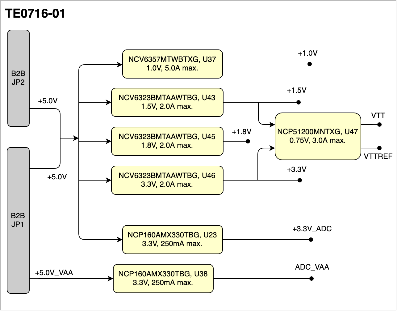 Image Added Image Added
|
|
Power-On Sequence
The TE0716 has only one common "PGOOD" signal (from U37, U43, U45 and U46), and there is no Enable for the board. You could control the startup of the board IC, by controlling the +5.0V and the +5.0V_VAA input signals only.
| Scroll Title |
|---|
| anchor | Figure_PWR_PS |
|---|
| title | Power Sequency |
|---|
|
| Scroll Ignore |
|---|
| draw.io Diagram |
|---|
| border | true |
|---|
| |
|---|
| diagramName | PWR-PS-TE0716-01 |
|---|
| simpleViewer | false |
|---|
| width | |
|---|
| links | auto |
|---|
| tbstyle | top |
|---|
| lbox | true |
|---|
| diagramWidth | 641 |
|---|
| revision | 4 |
|---|
|
|
| Scroll Only |
|---|
 Image Added Image Added
|
|
Voltage Monitor Circuit
The TE0716 has also a Voltage Monitor IC. It keeps nRST signal low if the FPGA core voltage (+1.0V) drops under 0.84V or the 3.3V power supply drops to 2.94V or less.
Power Good signal is unique and comes from the power supplies IC U37, U43, U45 and U46, as you can see in the previous section "Power-On Sequence", and also could make nRST to remain low until PGOOD is high.
See also "Reset process." section in "Configuration Signals" for additional information.
Power Supply
Power supply with minimum current capability of xx A for system startup is recommended.
Power Consumption
...
| anchor | Table_PWR_PC |
|---|
| title | Power Consumption |
|---|
...
* TBD - To Be Determined
...
| Scroll Title |
|---|
| anchor | Figure_PWR_PDVMC |
|---|
| title | Power DistributionVoltage Monitor Circuit |
|---|
|
| Scroll Ignore |
|---|
Create DrawIO object here: Attention if you copy from other page, objects are only linked. |
| Scroll Only |
|---|
image link to the generate DrawIO PNG file of this page. This is a workaround until scroll pdf export bug is fixed |
|
...
|
|---|
| draw.io Diagram |
|---|
| border | false |
|---|
| |
|---|
| diagramName | PWR-PM-TE0716-01 |
|---|
| simpleViewer | false |
|---|
| width | |
|---|
| links | auto |
|---|
| tbstyle | hidden |
|---|
| diagramDisplayName | |
|---|
| lbox | true |
|---|
| diagramWidth | 641 |
|---|
| revision | 3 |
|---|
|
|
| Scroll Only |
|---|
 Image Added Image Added
|
|
Power Rails
| Scroll Title |
|---|
| anchor | FigureTable_PWR_PSPR |
|---|
| title | Power Sequency |
|---|
| | Scroll Ignore |
|---|
Create DrawIO object here: Attention if you copy from other page, objects are only linked. |
| Scroll Only |
|---|
image link to the generate DrawIO PNG file of this page. This is a workaround until scroll pdf export bug is fixed |
Voltage Monitor Circuit
...
| anchor | Figure_PWR_VMC |
|---|
| title | Voltage Monitor Circuit |
|---|
| Scroll Ignore |
|---|
Create DrawIO object here: Attention if you copy from other page, objects are only linked. |
| Scroll Only |
|---|
image link to the generate DrawIO PNG file of this page. This is a workaround until scroll pdf export bug is fixed |
|
| Scroll Table Layout |
|---|
| orientation | portrait |
|---|
| sortDirection | ASC |
|---|
| repeatTableHeaders | default |
|---|
| style | |
|---|
| widths | |
|---|
| sortByColumn | 1 |
|---|
| sortEnabled | false |
|---|
| cellHighlighting | true |
|---|
|
| Power Rail Name | B2B Connector JP1 Pin | B2B Connector JP2 Pin | Direction | Notes |
|---|
| +5.0V | 1, 3, 5 | 1, 3, 5 | Input | Main Supply voltage from the carrier board | | +5.0V_VAA | 43, 44 | - | Input | Analog Supply voltage from the carrier board | | +3.3V (VREF_JTAG) | - | 5 | Output | JTAG reference voltage. |
|
Bank Voltages
...
| Scroll Title |
|---|
| anchor | Table_PWR_PRBV |
|---|
| title | Module power railsZynq SoC bank voltages. |
|---|
|
| Scroll Table Layout |
|---|
| orientation | portrait |
|---|
| sortDirection | ASC |
|---|
| repeatTableHeaders | default |
|---|
| style | |
|---|
| widths | |
|---|
| sortByColumn | 1 |
|---|
| sortEnabled | false |
|---|
| cellHighlighting | true |
|---|
|
Power Rail B2B ConnectorJM1 Pin B2B Connector JM2 Pin | B2B Connector JM3 Pin | Direction | Notes | |
Bank Voltages
| Notes |
|---|
| PS BANK 500 | VCCO_MIO0_500 | +3.3V | - | | PS BANK 501 | VCCO_MIO0_501 | +1.8V | - | | PS BANK 502 | VCCO_DDR_502 | +1.5V | - | | PL BANK 0 HR | VCCO_0 | +3.3V | - | | PL BANK 13 HR | VCCO_13 | +3.3V | - | | PL BANK 33 HR | VCCO_33 | +3.3V | - | | PL BANK 34 HR | VCCO_34 | +3.3V | - | | PL BANK 35 HR | VCCO_35 | +3.3V | - |
|
| Scroll Title |
|---|
| anchor | Table_PWR_BV |
|---|
| title | Zynq SoC bank voltages. |
|---|
|
| Scroll Table Layout |
|---|
|
| orientation | portrait |
|---|
| sortDirection | ASC |
|---|
| repeatTableHeaders | default |
|---|
style | widths | | sortByColumn | 1 |
|---|
| sortEnabled | false |
|---|
| cellHighlighting | true |
|---|
Board to Board Connectors
| Page properties |
|---|
|
- This section is optional and only for modules.
use "include page" macro and link to the general B2B connector page of the module series, For example: 6 x 6 SoM LSHM B2B Connectors
| Include Page |
|---|
| PD:6 x 6 SoM LSHM B2B ConnectorsPD: |
|---|
| 6 x 6 SoM LSHM B2B Connectors |
|---|
|
|
? x ? modules use two or three Samtec Micro Tiger Eye Connector on TE0716 module use two 61083 BergStak® 0.8mm Plug Connectors on the bottom side.
3 x REF-??????? (compatible to ????????), (?? pins, ?? per row)- Part Number: 61083-121402LF (compatible with 61082 Receptacle).
- Operating Temperature: -
- 40°C to +125°C.
- Current Rating:
- 0.8A per Contact.
- Number of Positions:
- 120 (60x per row)
- Number of Rows:
Technical Specifications
Absolute Maximum Ratings
| Scroll Title |
|---|
| anchor | Table_TS_AMR |
|---|
| title | PS absolute Absolute maximum ratings |
|---|
|
| Scroll Table Layout |
|---|
| orientation | portrait |
|---|
| sortDirection | ASC |
|---|
| repeatTableHeaders | default |
|---|
style | widths | | sortByColumn | 1 |
|---|
| sortEnabled | false |
|---|
| cellHighlighting | true |
|---|
|
|
| Symbols | Description | Min | Max | Unit |
|---|
V | V | V | V | V | V | V | V | | portrait |
|---|
| sortDirection | ASC |
|---|
| repeatTableHeaders | default |
|---|
| style | |
|---|
| widths | |
|---|
| sortByColumn | 1 |
|---|
| sortEnabled | false |
|---|
| cellHighlighting | true |
|---|
|
| Symbols | Description | Min | Max | Unit | Reference |
|---|
| +5.0V | Main Supply voltage from the carrier board | -0.3 | 6.0 | V | NCV6357 Datasheet
NCV6323 Datasheet
NCP160 Datasheet |
| +5.0V_VAA | Analog Supply voltage from the carrier board | -0.3 | 6.0 | V | NCP160 Datasheet |
| MIO 500 | I/O input voltage for MIO bank 500 | -0.4 | 3.85 | V | Xilinx DS187 Datasheet |
| MIO 501 | I/O input voltage for MIO bank 501 | -0.4 | 2.35 | V | Xilinx DS187 Datasheet |
| PL HR | I/O input voltage for HR banks | -0.4 | 3.85 | V | Xilinx DS187 Datasheet |
| ADCx_P/N | I/O input voltage for ADCs analog inputs | -0.3 | 3.63 | V | NCD98011 Datasheet |
Recommended Operating Conditions
...
| Scroll Title |
|---|
| anchor | Table_TS_ROC |
|---|
| title | Recommended operating conditions. |
|---|
|
| Scroll Table Layout |
|---|
| orientation | portrait |
|---|
| sortDirection | ASC |
|---|
| repeatTableHeaders | default |
|---|
| style | |
|---|
| widths | |
|---|
| sortByColumn | 1 |
|---|
| sortEnabled | false |
|---|
| cellHighlighting | true |
|---|
|
| Parameter | Min | Max | Units | Reference Document |
|---|
+5.0V Main Supply input voltage
from the carrier board | 4.0 | 5.5 | V | 7WB3125 Datasheet NCV6357 Datasheet NCV6323 Datasheet NCP160 Datasheet | +5.0V_VAA Analog Supply input voltage
from the carrier board | 3.75 | 5.5 | V | NCP160 Datasheet | | I/O input voltage for MIO bank 500 | -0.2 | 3.5See ???? datasheets. | V | Xilinx DS187 Datasheet | | I/O input voltage for MIO bank 501 | -0.2 | 2.0 | V | Xilinx DS187 Datasheet | | I/O input voltage for HR banks | -0.2 | 3.5 | V | Xilinx DS187 Datasheet | | I/O input voltage for ADCs analog inputs | -0.2 | 3.4 | V | NCD98011 Datasheet | See Xilinx ???? datasheet. | V | See Xilinx ???? datasheet. | V | See Xilinx ???? datasheet. | V | See Xilinx ???? datasheet. | V | See Xilinx ???? datasheet. | V | See Xilinx ???? datasheet. | °C | See Xilinx ???? datasheet. | °C | See Xilinx ???? datasheet. |
|
Physical Dimensions
Module size: ?? 45 mm × ?? 65 mm. Please download the assembly diagram for exact numbers.
Mating height with standard 61982 receptacle connectors: ? mm5mm, 7mm, 13mm and 17mm stack heights.
PCB thickness:
...
| Page properties |
|---|
|
In 'Physical Dimension' section, top and bottom view of module must be inserted, information regarding physical dimensions can be obtained through webpage for product in Shop.Trenz, (Download> Documents> Assembly part) for every SoM. For Example: for Module TE0728, Physical Dimension information can be captured by snipping tools from the link below: https://www.trenz-electronic.de/fileadmin/docs/Trenz_Electronic/Modules_and_Module_Carriers/5.2x7.6/TE0745/REV02/Documents/AD-TE0745-02-30-1I.PDF
|
...
| Scroll Title |
|---|
| anchor | Figure_TS_PD |
|---|
| title | Physical Dimension |
|---|
|
| Scroll Ignore |
|---|
| draw.io Diagram |
|---|
| border | false |
|---|
| |
|---|
| diagramName | PD-TE0716-01 |
|---|
| simpleViewer | false |
|---|
| width | |
|---|
| links | auto |
|---|
| tbstyle | hidden |
|---|
| diagramDisplayName | |
|---|
| lbox | true |
|---|
| diagramWidth | 641 |
|---|
| revision | 2 |
|---|
|
Create DrawIO object here: Attention if you copy from other page, objects are only linked. |
| Scroll Only |
|---|
| scroll-pdf | true |
|---|
| scroll-office | true |
|---|
| scroll-chm | true |
|---|
| scroll-docbook | true |
|---|
| scroll-eclipsehelp | true |
|---|
| scroll-epub | true |
|---|
| scroll-html | true |
|---|
| image link to the generate DrawIO PNG file of this page. This is a workaround until scroll pdf export bug is fixed Image Added Image Added |
|
Currently Offered Variants
| Scroll Title |
|---|
| anchor | Table_VCP_SO |
|---|
| title | Trenz Electronic Shop Overview |
|---|
|
| Scroll Table Layout |
|---|
| orientation | portrait |
|---|
| sortDirection | ASC |
|---|
| repeatTableHeaders | default |
|---|
| style | |
|---|
| widths | |
|---|
| sortByColumn | 1 |
|---|
| sortEnabled | false |
|---|
| cellHighlighting | true |
|---|
|
|
...
| Scroll Title |
|---|
| anchor | Table_RH_HRH |
|---|
| title | Hardware Revision History |
|---|
|
| Scroll Table Layout |
|---|
| orientation | portrait |
|---|
| sortDirection | ASC |
|---|
| repeatTableHeaders | default |
|---|
| style | |
|---|
| widths | |
|---|
| sortByColumn | 1 |
|---|
| sortEnabled | false |
|---|
| cellHighlighting | true |
|---|
|
| Date | Revision | Changes | Documentation Link |
|---|
| 2020-10-25 | REV01 | Initial Release | REV01 |
|
Hardware revision number can be found on the PCB board together with the module model number separated by the dash.model number separated by the dash.
| Scroll Title |
|---|
| anchor | Figure_RV_HRN |
|---|
| title | Board hardware revision number. |
|---|
|
| Scroll Ignore |
|---|
| draw.io Diagram |
|---|
| border | false |
|---|
| |
|---|
| diagramName | RH-HRN-TE0716-01 |
|---|
| simpleViewer | false |
|---|
| width | |
|---|
| links | auto |
|---|
| tbstyle | hidden |
|---|
| diagramDisplayName | |
|---|
| lbox | true |
|---|
| diagramWidth | 545 |
|---|
| revision | 4 |
|---|
|
|
| Scroll Only |
|---|
 Image Added Image Added
|
|
| Scroll Title |
|---|
| anchor | Figure_RV_HRN |
|---|
| title | Board hardware revision number. |
|---|
|
| Scroll Ignore |
|---|
Create DrawIO object here: Attention if you copy from other page, objects are only linked. |
| Scroll Only |
|---|
image link to the generate DrawIO PNG file of this page. This is a workaround until scroll pdf export bug is fixed |
|
Document Change History
| Page properties |
|---|
|
- Note this list must be only updated, if the document is online on public doc!
- It's semi automatically, so do following
Add new row below first Copy "Page Information Macro(date)" Macro-Preview, Metadata Version number, Author Name and description to the empty row. Important Revision number must be the same as the Wiki document revision number Update Metadata = "Page Information Macro (current-version)" Preview+1 and add Author and change description. --> this point is will be deleted on newer pdf export template - Metadata is only used of compatibility of older exports
|
...
| Scroll Title |
|---|
| anchor | Table_RH_DCH |
|---|
| title | Document change history. |
|---|
|
| Scroll Table Layout |
|---|
| orientation | portrait |
|---|
| sortDirection | ASC |
|---|
| repeatTableHeaders | default |
|---|
| style | |
|---|
| widths | |
|---|
| sortByColumn | 1 |
|---|
| sortEnabled | false |
|---|
| cellHighlighting | true |
|---|
|
| Date | Revision | Contributor | Description |
|---|
| Page info |
|---|
| infoType | Modified date |
|---|
| dateFormat | yyyy-MM-dd |
|---|
| type | Flat |
|---|
|
| | Page info |
|---|
| infoType | Current version |
|---|
| prefix | v. |
|---|
| type | Flat |
|---|
| showVersions | false |
|---|
|
| | Page info |
|---|
| infoType | Modified by |
|---|
| type | Flat |
|---|
| showVersions | false |
|---|
|
change list | | | 2020-10-30 | v.85 | Guillermo Herrera | | -- | all | | Page info |
|---|
| infoType | Modified users |
|---|
| type | Flat |
|---|
| showVersions | false |
|---|
|
| |
|
...