...
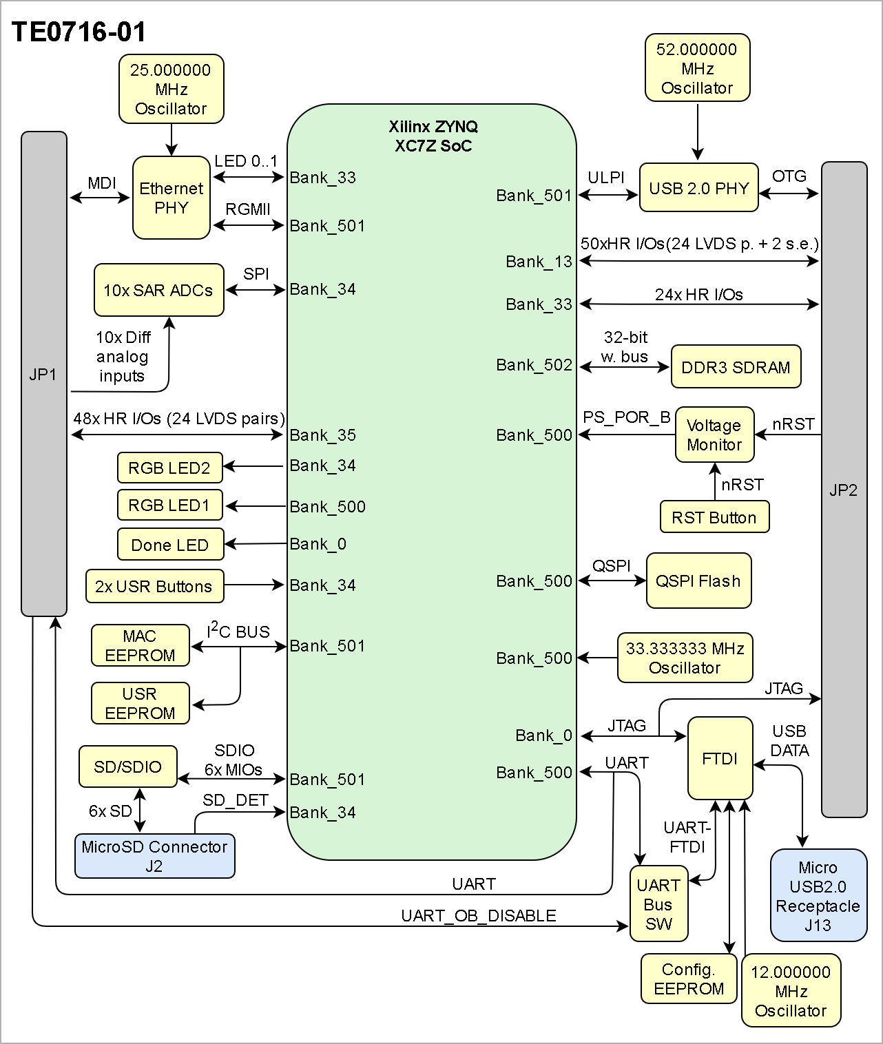
| Scroll Title |
|---|
| anchor | Figure_OV_BD |
|---|
| title | TE0716-01 block diagram |
|---|
|
| Scroll Ignore |
|---|
| draw.io Diagram |
|---|
| border | false |
|---|
| |
|---|
| diagramName | DB-TE0716-01 |
|---|
| simpleViewer | false |
|---|
| width | |
|---|
| links | auto |
|---|
| tbstyle | hidden |
|---|
| diagramDisplayName | |
|---|
| lbox | true |
|---|
| diagramWidth | 641 |
|---|
| revision | 1819 |
|---|
|
|
| Scroll Only |
|---|
|
|
Main Components
...
| Scroll Title |
|---|
| anchor | Table_OV_IDS |
|---|
| title | Initial delivery state of programmable devices on the module |
|---|
|
| Scroll Table Layout |
|---|
| orientation | portrait |
|---|
| sortDirection | ASC |
|---|
| repeatTableHeaders | default |
|---|
| style | |
|---|
| widths | |
|---|
| sortByColumn | 1 |
|---|
| sortEnabled | false |
|---|
| cellHighlighting | true |
|---|
|
Storage device name | IC Designator | Content | Notes |
|---|
Quad SPI Flash | U7 | Empty | - | | 512Kb Serial EEPROM | U21 | Empty | - | | 2Kb 24AA025E48 EEPROM | U24 | Pre-programmed globally unique, 48-bit node address (MAC). | - | | 4Kb M93C66-R EEPROM | U40 | Xilinx JTAG Programmer License- | For FTDI IC only (U39). |
|
Configuration Signals
| Page properties |
|---|
|
- Overview of Boot Mode, Reset, Enables.
|
...
The PWM signals are connected to B2B connector JP2. All this digital signals are connected to PL Bank 33 (except for PWM_6_H and PWM_6_L which are connected to PL Bank 13). This These signals could be also used as normal single ended I/Os.
...
- Part number: S25FL256SAGBHI20*
- Supply voltage: 3.3V (2.7V - 3.6V).
- Speed: 133MHz max.*
- Temperature: Industrial Range -40°C to +85°C.
Notes: * standard number/value but depends on assembly version.
| Scroll Title |
|---|
| anchor | Table_OBP_SPI |
|---|
| title | Quad SPI interface MIOs and pins |
|---|
|
| Scroll Table Layout |
|---|
| orientation | portrait |
|---|
| sortDirection | ASC |
|---|
| repeatTableHeaders | default |
|---|
| style | |
|---|
| widths | |
|---|
| sortByColumn | 1 |
|---|
| sortEnabled | false |
|---|
| cellHighlighting | true |
|---|
|
| MIO Pin | Schematic | U7 Pin | Notes |
|---|
| MIO1 | SPI-CS | CS# | - | | MIO3 | SPI-DQ1/M1 | SO/IO1 | - | | MIO4 | SPI-DQ2/M2 | WP#/IO2 | - | | MIO2 | SPI-DQ3/M3 | HOLD#/IO3 | - | | MIO5 | SPI-DQO/M0 | SI/IO0 | - | | MIO6 | SPI-SCK/M4 | SCK | - |
|
...
| Scroll Title |
|---|
| anchor | Table_OBP_I2C_EEPROM |
|---|
| title | I2C address for EEPROM |
|---|
|
| Scroll Table Layout |
|---|
| orientation | portrait |
|---|
| sortDirection | ASC |
|---|
| repeatTableHeaders | default |
|---|
| style | |
|---|
| widths | |
|---|
| sortByColumn | 1 |
|---|
| sortEnabled | false |
|---|
| cellHighlighting | true |
|---|
|
| I2C Device | I2C Address | Designator | Notes |
|---|
| 2K Serial EEPROMs with EUI-48™ | 0xA6 (write)
0xA7 (read)
0x53 (7bit) | U24 | - | | 512Kb Serial EEPROM0xA0 (write) | 0xA1 (read)
0x50 (7bit) | U21 | - |
|
ADCs
The TE0716 module has 10x 12-Bit Low Power SAR Analog-to-Digital Converter, fully differential input, signed output, with SPI−compatible interface (NCD98011), which are connected to the FPGA PL BANK34.
...
| Scroll Title |
|---|
| anchor | Table_OBP_ADC |
|---|
| title | ADC to PL interface PL and pins |
|---|
|
| Scroll Table Layout |
|---|
| orientation | portrait |
|---|
| sortDirection | ASC |
|---|
| repeatTableHeaders | default |
|---|
| style | |
|---|
| widths | |
|---|
| sortByColumn | 1 |
|---|
| sortEnabled | false |
|---|
| cellHighlighting | true |
|---|
|
| Designator | Schematic | PL Pin | Notes |
|---|
| U1 | S0_CLK S0_CSN S0_OUT | J18 J16 K18 | 3.3V Max Voltage on any pin. | | U2 | S5_CLK S5_CSN S5_OUT | M21 T16 T17 | 3.3V Max Voltage on any pin. | | U3 | S1_CLK S1_CSN S1_OUT | L18 J21 L19 | 3.3V Max Voltage on any pin. | | U4 | S6_CLK S6_CSN S6_OUT | J22 K21 J20 | 3.3V Max Voltage on any pin. | | U10 | S2_CLK S2_CSN S2_OUT | M22 R21 R20 | 3.3V Max Voltage on any pin. | | U11 | S7_CLK S7_CSN S7_OUT | L22 M20 M19 | 3.3V Max Voltage on any pin. | | U15 | S3_CLK S3_CSN S3_OUT | J17 J15 L17 | 3.3V Max Voltage on any pin. | | U16 | S8_CLK S8_CSN S8_OUT | M17 N18 N17 | 3.3V Max Voltage on any pin. | | U17 | S4_CLK S4_CSN S4_OUT | P17 L21 P18 | 3.3V Max Voltage on any pin. | | U19 | S9_CLK S9_CSN S9_OUT | K15 P21 P20 | 3.3V Max Voltage on any pin. |
|
...
| Scroll Title |
|---|
| anchor | Table_OBP_ETH |
|---|
| title | Ethernet PHY to Zynq SoC connections |
|---|
|
| Scroll Table Layout |
|---|
| orientation | portrait |
|---|
| sortDirection | ASC |
|---|
| repeatTableHeaders | default |
|---|
| style | |
|---|
| widths | |
|---|
| sortByColumn | 1 |
|---|
| sortEnabled | false |
|---|
| cellHighlighting | true |
|---|
|
| U8 Pin | Signal Name | Connected to | Signal Description | Note |
|---|
TX_CLK | ETH-TXCK | MIO16 | RGMII Transmit Clock | - | TXD[0..3] | ETH-TXD0..3 | MIO17..20 | RGMII Transmit Data
| - | TX_CTRL | ETH-TXCTL | MIO21 | RGMII Transmit Control | - | RX_CLK | ETH-RXCK | MIO22 | RGMII Receive Clock | - | RXD[0..3] | ETH-RXD0..3 | MIO23..26 | RGMII Receive Data | - | RX_CTRL | ETH-RXCTL | MIO27 | RGMII Receive Control | - | MDC | ETH-MDC | MIO52 | Management data clock reference | - | MDIO | ETH-MDIO | MIO53 | Management data | - | RESETn | PHY-RST | MIO51, U18 | Hardware reset. Active low. | Shared with U18 (RESETB) USB | MDIP[0..3] MDIN[0..3] | PHY_MDI0..3_P
PHY_MDI0..3_N | JP1 | Media Dependent Interface | - | XTAL_IN | ETH-CLK | U9 | Reference Clock Input | see also Clock Sources section | LED[0..1] | PHY_LED0..1 | FPGA BANK 33 | LED output | - |
|
...
| Scroll Title |
|---|
| anchor | Table_OBP_USB |
|---|
| title | USB PHY to Zynq SoC connections |
|---|
|
| Scroll Table Layout |
|---|
| orientation | portrait |
|---|
| sortDirection | ASC |
|---|
| repeatTableHeaders | default |
|---|
| style | |
|---|
| widths | |
|---|
| sortByColumn | 1 |
|---|
| sortEnabled | false |
|---|
| cellHighlighting | true |
|---|
|
| U18 Pin | Signal Name | Connected to | Signal Description | Note |
|---|
CLKOUT | OTG-CLK | MIO36 | ULPI Output Clock | - | DATA[0..3] | OTG-DATA0..3 | MIO32..35 | ULPI bi-directional data bus | - | DATA[4] | OTG-DATA4 | MIO28 | ULPI bi-directional data bus | - | DATA[5..7] | OTG-DATA5..7 | MIO37..39 | ULPI bi-directional data bus | - | DIR | OTG-DIR | MIO29 | Controls the direction of the data bus | - | STP | OTG-STP | MIO30 | terminates transfers PHY input | - | NXT | OTG-NXT | MIO31 | control data flow into and out of the PHY | - | RESETB | PHY-RST | MIO51, U8 | reset and suspend the PHY. Active low. | Shared with U8 (RESETn) Ethernet | DP | USB_OTG_D_P | JP2-64 | D+ pin of the USB cable | 3.3V Voltage level | DM | USB_OTG_D_N | JP2-65 | D- pin of the USB cable | 3.3V Voltage level | ID | USB_OTG_ID | JP2-66 | ID pin of the USB cable | 3.3V Voltage level | CPEN | USB_VBUS_EN | JP2-67 | Controls the external VBUS power switch | 3.3V Voltage level | VBUS | USB_VBUS | JP2-68 | For RVBUS connection | Max. voltage: 5.5V | REFCLK | OTG-RCLK | U14 | ULPI clock input | see also Clock Sources section |
|
...
| Scroll Title |
|---|
| anchor | Table_OBP_FTDI |
|---|
| title | USB FTDI to Zynq SoC connections |
|---|
|
| Scroll Table Layout |
|---|
| orientation | portrait |
|---|
| sortDirection | ASC |
|---|
| repeatTableHeaders | default |
|---|
| style | |
|---|
| widths | |
|---|
| sortByColumn | 1 |
|---|
| sortEnabled | false |
|---|
| cellHighlighting | true |
|---|
|
| U39 Pin | Signal Name | Connected to | Signal Description | Note |
|---|
| DP | D_JTAG_P | J13-2 | USB Data Signal Plus | 3.3V Voltage level | | DM | D_JTAG_N | J13-3 | USB Data Signal Minus | 3.3V Voltage level | | ADBUS0 | TCK | JP2-8,
TCK_0 (FPGA PL BANK 0) | Clock Signal Output | 3.3V Voltage level.
MPSSE Mode | | ADBUS1 | TDI | JP2-11,
TDI_0 (FPGA PL BANK 0) | Serial Data Output | 3.3V Voltage level.
MPSSE Mode | | ADBUS2 | TDO | JP2-10,
TDO_0 (FPGA PL BANK 0) | Serial Data Input | 3.3V Voltage level.
MPSSE Mode | | ADBUS3 | TMS | JP2-7,
TMS_0 (FPGA PL BANK 0) | Output Signal Select | 3.3V Voltage level.
MPSSE Mode | | BDBUS0 | UART_TX_OB | U36-5 | Asynchronous serial TXD | U36-3 Bus Switch pin connects later this signal to UART_RX_ZYNQ when UART_OB_DISABLE is low or floating. | | BDBUS1 | UART_RX_OB | U36-6 | Asynchronous serial RXD | U36-2 Bus Switch pin connects later this signal to UART_TX_ZYNQ when UART_OB_DISABLE is low or floating. | | OSCI | OSCI |
| Oscillator input | - | | EECS, EECLK, EEDATA | EECS, EECLK, EEDATA | U40-1..3 | EEPROM interface | - | | - | UART_OB_DISABLE | JP1-11 | Enable signal of the FTDI-PS_UART Bus Switch U36. | Active Low!. |
|
...
Power supply with minimum current capability of 3.0 A (TBD*) for system startup is recommended.
* TBD - To Be Determined
Power Consumption
| Scroll Title |
|---|
| anchor | Table_PWR_PC |
|---|
| title | Power Consumption |
|---|
|
| Scroll Table Layout |
|---|
| orientation | portrait |
|---|
| sortDirection | ASC |
|---|
| repeatTableHeaders | default |
|---|
| style | |
|---|
| widths | |
|---|
| sortByColumn | 1 |
|---|
| sortEnabled | false |
|---|
| cellHighlighting | true |
|---|
|
| Power Input Pin | Typical Current |
|---|
| +5.0V | TBD* | | +5.0V_VAA | less than 250mA (TBD*) |
|
* TBD - To Be Determined
...
| Scroll Title |
|---|
| anchor | Figure_PWR_PD |
|---|
| title | Power Distribution |
|---|
|
| Scroll Ignore |
|---|
| draw.io Diagram |
|---|
| border | false |
|---|
| |
|---|
| diagramName | PWR-PD-TE0716-01 |
|---|
| simpleViewer | false |
|---|
| width | |
|---|
| links | auto |
|---|
| tbstyle | hidden |
|---|
| diagramDisplayName | |
|---|
| lbox | true |
|---|
| diagramWidth | 643 |
|---|
| revision | 2 |
|---|
|
|
| Scroll Only |
|---|
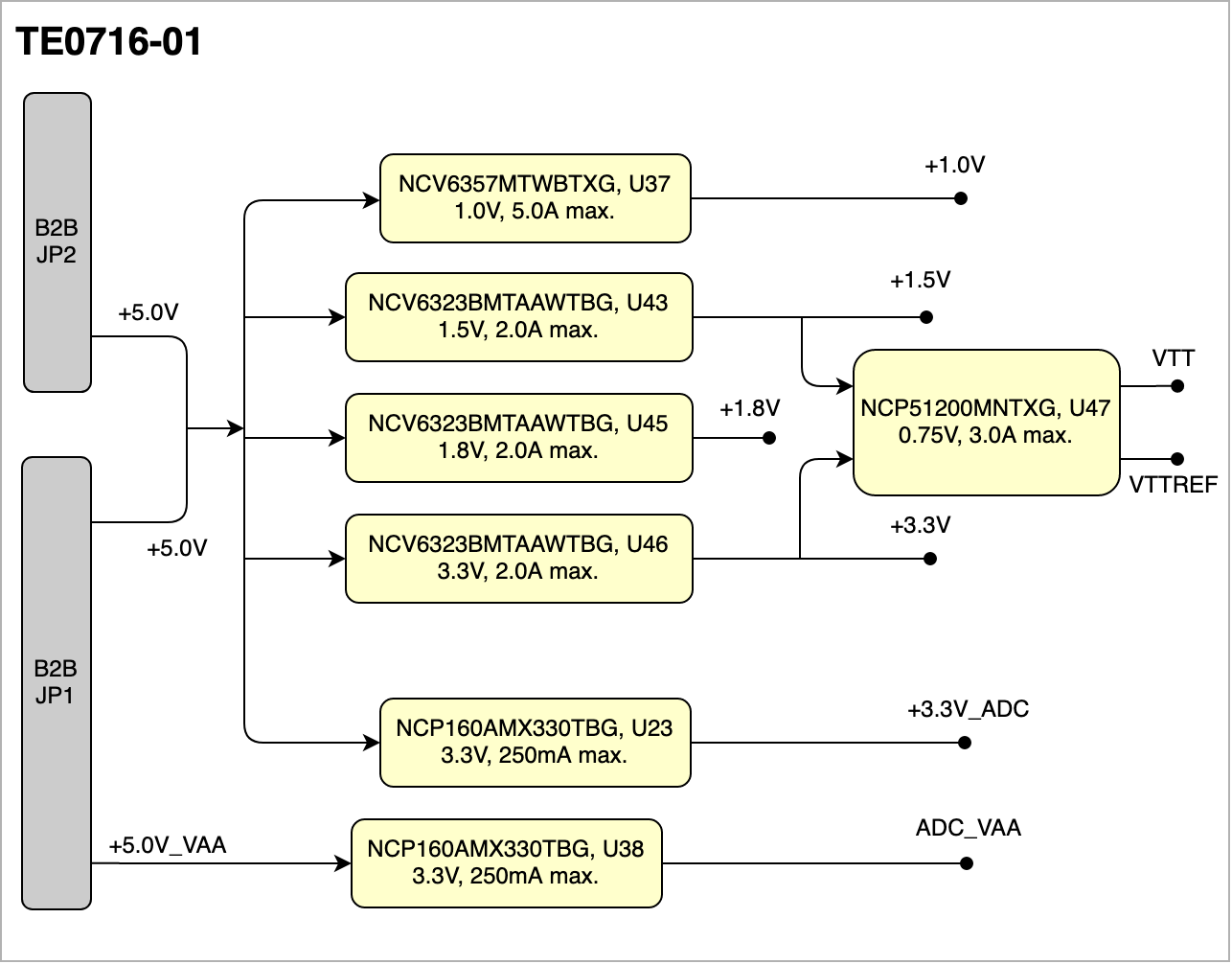 Image Modified Image Modified
|
|
Power-On Sequence
The TE0716 has only one common "PGOOD" signal (from U37, U43, U45 and U46), and there is no Enable for the board. You could control the startup of the board IC, by controlling the +5.0V and the +5.0V_VAA input signals only.
| Scroll Title |
|---|
| anchor | Figure_PWR_PS |
|---|
| title | Power Sequency |
|---|
|
| Scroll Ignore |
|---|
| draw.io Diagram |
|---|
| border | true |
|---|
| |
|---|
| diagramName | PWR-PS-TE0716-01 |
|---|
| simpleViewer | false |
|---|
| width | |
|---|
| links | auto |
|---|
| tbstyle | top |
|---|
| lbox | true |
|---|
| diagramWidth | 641 |
|---|
| revision | 4 |
|---|
|
|
| Scroll Only |
|---|
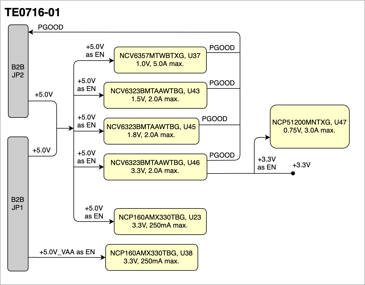 Image Added Image Added
|
|
Voltage Monitor Circuit
The TE0716 has also a Voltage Monitor IC. It keeps nRST signal low if the FPGA core voltage (+1.0V) drops under 0.84V or the 3.3V power supply drops to 2.94V or less.
Power Good signal is unique and comes from the power supplies IC U37, U43, U45 and U46, as you can see in the previous section "Power-On Sequence", and also could make nRST to remain low until PGOOD is high.
See also "Reset process." section in "Configuration Signals" for additional information.
| Scroll Title |
|---|
| anchor | Figure_PWR_VMC |
|---|
| title | Voltage Monitor Circuit |
|---|
|
| Scroll Ignore |
|---|
| draw.io Diagram |
|---|
| border | false |
|---|
| |
|---|
| diagramName | PWR-PM-TE0716-01 |
|---|
| simpleViewer |
|---|
|
|
|
| Scroll Title |
|---|
| anchor | Figure_PWR_PS |
|---|
| title | Power Sequency |
|---|
|
| Scroll Ignore |
|---|
| draw.io Diagram |
|---|
| border | true |
|---|
| diagramName | PWR-PS-TE0716-01 |
|---|
| simpleViewer | false |
|---|
| width | |
|---|
| links | auto |
|---|
| tbstyle | hiddentop |
|---|
| diagramDisplayName | |
|---|
| lbox | true |
|---|
| diagramWidth | 641 |
|---|
| revision | 3 |
|---|
|
|
| Scroll Only |
|---|
Image Removed |
|
Voltage Monitor Circuit
| Scroll Title |
|---|
| anchor | Figure_PWR_VMC |
|---|
| title | Voltage Monitor Circuit |
|---|
|
| Scroll Ignore |
|---|
Create DrawIO object here: Attention if you copy from other page, objects are only linked. |
scroll-only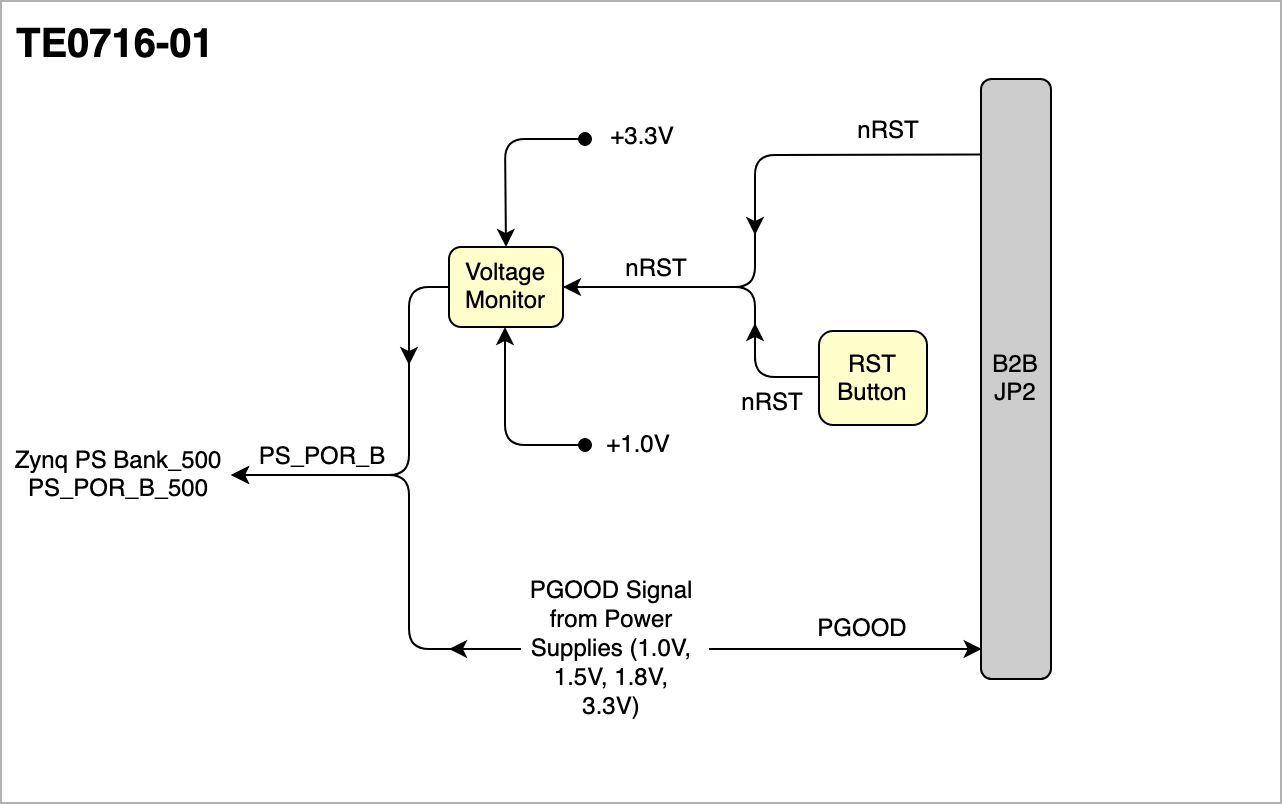 Image Added Image Added
|
|
Power Rails
| Scroll Title |
|---|
| anchor | Table_PWR_PR |
|---|
| title | Module power rails. |
|---|
|
| Scroll Table Layout |
|---|
| orientation | portrait |
|---|
| sortDirection | ASC |
|---|
| repeatTableHeaders | default |
|---|
| style | |
|---|
| widths | |
|---|
| sortByColumn | 1 |
|---|
| sortEnabled | false |
|---|
| cellHighlighting | true |
|---|
|
| Power Rail Name | B2B Connector JP1 Pin | B2B Connector JP2 Pin | Direction | Notes |
|---|
| +5.0V | 1, 23, 35 | 1, 23, 35 | Input | Main Supply voltage from the carrier board | | +5.0V_VAA | 43, 44 | - | Input | Analog Supply voltage from the carrier board | | +3.3V (VREF_JTAG) | - | 5 | Output | JTAG reference voltage. |
|
...
| Page properties |
|---|
|
- This section is optional and only for modules.
use "include page" macro and link to the general B2B connector page of the module series, For example: 6 x 6 SoM LSHM B2B Connectors
| Include Page |
|---|
| PD:6 x 6 SoM LSHM B2B ConnectorsPD: |
|---|
| 6 x 6 SoM LSHM B2B Connectors |
|---|
|
|
...
| Scroll Title |
|---|
| anchor | Table_TS_AMR |
|---|
| title | PS absolute Absolute maximum ratings |
|---|
|
| Scroll Table Layout |
|---|
| orientation | portrait |
|---|
| sortDirection | ASC |
|---|
| repeatTableHeaders | default |
|---|
| style | |
|---|
| widths | |
|---|
| sortByColumn | 1 |
|---|
| sortEnabled | false |
|---|
| cellHighlighting | true |
|---|
|
| Symbols | Description | Min | Max | Unit | Reference |
|---|
| +5.0V | Main Supply voltage from the carrier board | -0.3 | 6.0 | V | NCV6357 Datasheet
NCV6323 Datasheet
NCP160 Datasheet | | +5.0V_VAA | Analog Supply voltage from the carrier board | -0.3 | 6.0 | V | NCP160 Datasheet | | MIO 500 | I/O input voltage for MIO bank 500 | -0.4 | 3.85 | V | Xilinx DS187 Datasheet | | MIO 501 | I/O input voltage for MIO bank 501 | -0.4 | 2.35 | V | Xilinx DS187 Datasheet | | PL HR | I/O input voltage for HR banks | -0.4 | 3.85 | V | Xilinx DS187 Datasheet | | ADCx_P/N | I/O input voltage for ADCs analog inputs | -0.3 | 3.63 | V | NCD98011 Datasheet |
|
...
| Scroll Title |
|---|
| anchor | Table_TS_ROC |
|---|
| title | Recommended operating conditions. |
|---|
|
| Scroll Table Layout |
|---|
| orientation | portrait |
|---|
| sortDirection | ASC |
|---|
| repeatTableHeaders | default |
|---|
| style | |
|---|
| widths | |
|---|
| sortByColumn | 1 |
|---|
| sortEnabled | false |
|---|
| cellHighlighting | true |
|---|
|
| Parameter | Min | Max | Units | Reference Document |
|---|
+5.0V Main Supply input voltage
from the carrier board | 4.0 | 5.5 | V | 7WB3125 Datasheet NCV6357 Datasheet NCV6323 Datasheet NCP160 Datasheet | +5.0V_VAA Analog Supply input voltage
from the carrier board | 3.75 | 5.5 | V | NCP160 Datasheet | | I/O input voltage for MIO bank 500 | -0.2 | 3.x5 | V | Xilinx DS187 Datasheet | | I/O input voltage for MIO bank 501 | -0.2 | 2.x0 | V | Xilinx DS187 Datasheet | | I/O input voltage for HR banks | -0.2 | 3.x5 | V | Xilinx DS187 Datasheet | | I/O input voltage for ADCs analog inputs | -0.2 | 3.x4 | V | NCD98011 Datasheet |
|
Physical Dimensions
...
| Scroll Title |
|---|
| anchor | Table_VCP_SO |
|---|
| title | Trenz Electronic Shop Overview |
|---|
|
| Scroll Table Layout |
|---|
| orientation | portrait |
|---|
| sortDirection | ASC |
|---|
| repeatTableHeaders | default |
|---|
| style | |
|---|
| widths | |
|---|
| sortByColumn | 1 |
|---|
| sortEnabled | false |
|---|
| cellHighlighting | true |
|---|
|
|
...
| Scroll Title |
|---|
| anchor | Figure_RV_HRN |
|---|
| title | Board hardware revision number. |
|---|
|
| Scroll Ignore |
|---|
| draw.io Diagram |
|---|
| border | false |
|---|
| |
|---|
| diagramName | RH-HRN-TE0716-01 |
|---|
| simpleViewer | false |
|---|
| width | |
|---|
| links | auto |
|---|
| tbstyle | hidden |
|---|
| diagramDisplayName | |
|---|
| lbox | true |
|---|
| diagramWidth | 545 |
|---|
| revision | 4 |
|---|
|
|
| Scroll Only |
|---|
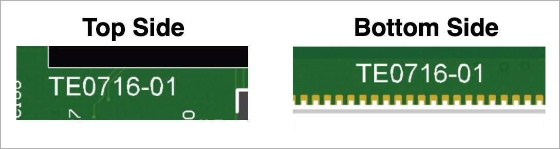 Image Added Image Added
| Create DrawIO object here: Attention if you copy from other page, objects are only linked. | | Scroll Only |
|---|
image link to the generate DrawIO PNG file of this page. This is a workaround until scroll pdf export bug is fixed |
|
Document Change History
| Page properties |
|---|
|
- Note this list must be only updated, if the document is online on public doc!
- It's semi automatically, so do following
Add new row below first Copy "Page Information Macro(date)" Macro-Preview, Metadata Version number, Author Name and description to the empty row. Important Revision number must be the same as the Wiki document revision number Update Metadata = "Page Information Macro (current-version)" Preview+1 and add Author and change description. --> this point is will be deleted on newer pdf export template - Metadata is only used of compatibility of older exports
|
...
| Scroll Title |
|---|
| anchor | Table_RH_DCH |
|---|
| title | Document change history. |
|---|
|
| Scroll Table Layout |
|---|
| orientation | portrait |
|---|
| sortDirection | ASC |
|---|
| repeatTableHeaders | default |
|---|
| style | |
|---|
| widths | |
|---|
| sortByColumn | 1 |
|---|
| sortEnabled | false |
|---|
| cellHighlighting | true |
|---|
|
| Date | Revision | Contributor | Description |
|---|
| Page info |
|---|
| infoType | Modified date |
|---|
| dateFormat | yyyy-MM-dd |
|---|
| type | Flat |
|---|
|
| | Page info |
|---|
| infoType | Current version |
|---|
| prefix | v. |
|---|
| type | Flat |
|---|
| showVersions | false |
|---|
|
| | Page info |
|---|
| infoType | Modified by |
|---|
| type | Flat |
|---|
| showVersions | false |
|---|
|
change list | | | 2020-10-30 | v.85 | Guillermo Herrera | | -- | all | | Page info |
|---|
| infoType | Modified users |
|---|
| type | Flat |
|---|
| showVersions | false |
|---|
|
| |
|
...