...
| Scroll Title |
|---|
| anchor | Table_SIP_ADCs |
|---|
| title | ADCs pins connection |
|---|
|
| Scroll Table Layout |
|---|
| orientation | portrait |
|---|
| sortDirection | ASC |
|---|
| repeatTableHeaders | default |
|---|
| style | |
|---|
| widths | |
|---|
| sortByColumn | 1 |
|---|
| sortEnabled | false |
|---|
| cellHighlighting | true |
|---|
|
ADC Signal | B2B Connector | Notes |
|---|
ADC0_P
ADC0_N | JP1-106..107 | SAR ADC, U1.
3.3V Max. Voltage on any pin. | ADC1_P
ADC1_N | JP1-46..47 | SAR ADC, U3.
3.3V Max. Voltage on any pin. | ADC2_P
ADC2_N | JP1-109..110 | SAR ADC, U10.
3.3V Max. Voltage on any pin. | ADC3_P
ADC3_N | JP1-49..50 | SAR ADC, U15.
3.3V Max. Voltage on any pin. | ADC4_P
ADC4_N | JP1-112..113 | SAR ADC, U17.
3.3V Max. Voltage on any pin. | ADC5_P
ADC5_N | JP1-52..53 | SAR ADC, U2.
3.3V Max. Voltage on any pin. | ADC6_P
ADC6_N | JP1-115..116 | SAR ADC, U4.
3.3V Max. Voltage on any pin. | ADC7_P
ADC7_N | JP1-55..56 | SAR ADC, U11.
3.3V Max. Voltage on any pin. | ADC8_P
ADC8_N | JP1-118..119 | SAR ADC, U16.
3.3V Max. Voltage on any pin. | ADC9_P
ADC9_N | JP1-58..59 | SAR ADC, U19.
3.3V Max. Voltage on any pin. |
|
PWM Interface
@Guillermo: Hier die JP2 Stecker Pins wo PWN rausgeführt wird
Micro USB -JTAG/UART
A microUSB-B connector (J13) is connected to the FTDI. It provides the ability to communicate to the PL FPGA via JTAG, as well as to the PS UART (UART 0).
Caution: because the TE0716 also provides UART and JTAG access to the FPGA through B2B connectors JP1 and JP2 respectively, ONLY ONE connection for UART, and ONLY ONE connection for JTAG, should be used at the time! (please read "UART Interface" and "JTAG Interface" above in the "Board to Board (B2B)" Section).
Micro SD Socket
...
The PWM signals are connected to B2B connector JP2. All this digital signals are connected to PL Bank 33 (except for PWM_6_H and PWM_6_L which are connected to PL Bank 13). This signals could be also used as normal single ended I/Os.
| Scroll Title |
|---|
| anchor | Table_SIP_PWMs |
|---|
| title | PWMs pins connection |
|---|
|
| Scroll Table Layout |
|---|
| orientation | portrait |
|---|
| sortDirection | ASC |
|---|
| repeatTableHeaders | default |
|---|
| style | |
|---|
| widths | |
|---|
| sortByColumn | 1 |
|---|
| sortEnabled | false |
|---|
| cellHighlighting | true |
|---|
|
PWM Signal | B2B Connector | Notes |
|---|
| PWM_0_H | JP2-103 | 3.3V Max. Voltage on any pin. | | PWM_0_L | JP2-104 | 3.3V Max. Voltage on any pin. | | PWM_1_H | JP243 | 3.3V Max. Voltage on any pin. | | PWM_1_L | JP2-44 | 3.3V Max. Voltage on any pin. | | PWM_10_H | JP2-118 | 3.3V Max. Voltage on any pin. | | PWM_10_L | JP2-119 | 3.3V Max. Voltage on any pin. | | PWM_11_H | JP2-58 | 3.3V Max. Voltage on any pin. | | PWM_11_L | JP2-59 | 3.3V Max. Voltage on any pin. | | PWM_2_H | JP2-106 | 3.3V Max. Voltage on any pin. | | PWM_2_L | JP2-107 | 3.3V Max. Voltage on any pin. | | PWM_3_H | JP2-46 | 3.3V Max. Voltage on any pin. | | PWM_3_L | JP2-47 | 3.3V Max. Voltage on any pin. | | PWM_4_H | JP2-109 | 3.3V Max. Voltage on any pin. | | PWM_4_L | JP2-110 | 3.3V Max. Voltage on any pin. | | PWM_5_H | JP2-49 | 3.3V Max. Voltage on any pin. | | PWM_5_L | JP2-50 | 3.3V Max. Voltage on any pin. | | PWM_6_H | JP2-112 | 3.3V Max. Voltage on any pin. | | PWM_6_L | JP2-113 | 3.3V Max. Voltage on any pin. | | PWM_7_H | JP2-52 | 3.3V Max. Voltage on any pin. | | PWM_7_L | JP2-53 | 3.3V Max. Voltage on any pin. | | PWM_8_H | JP2-115 | 3.3V Max. Voltage on any pin. | | PWM_8_L | JP2-116 | 3.3V Max. Voltage on any pin. | | PWM_9_H | JP2-55 | 3.3V Max. Voltage on any pin. | | PWM_9_L | JP2-56 | 3.3V Max. Voltage on any pin. |
|
Micro USB -JTAG/UART
A microUSB-B connector (J13) is connected to the FTDI. It provides the ability to communicate to the PL FPGA via JTAG, as well as to the PS UART (UART 0).
Caution: because the TE0716 also provides UART and JTAG access to the FPGA through B2B connectors JP1 and JP2 respectively, ONLY ONE connection for UART, and ONLY ONE connection for JTAG, should be used at the time! (please read "UART Interface" and "JTAG Interface" above in the "Board to Board (B2B)" Section).
Micro SD Socket
A microSD™ card connector (J2) is connected via U35 (SD/SDIO Multiplexer - Level Translator) to Zynq PS (Bank501/SDIO 0). It is a Push-On/Push-Off socket type, and work with a voltage level of 3.3V.
MIO Pins
| Page properties |
|---|
|
you must fill the table below with group of MIOs which are connected to a specific components or peripherals, you do not have to specify pins in B2B, Just mention which B2B is connected to MIOs. The rest is clear in the Schematic. Example: | MIO Pin | Connected to | B2B | Notes |
|---|
| MIO12...14 | SPI_CS , SPI_DQ0... SPI_DQ3 SPI_SCK | J2 | QSPI |
|
PS MIO banks 500/501 signal connections to interface.
| Scroll Title |
|---|
| anchor | Table_SIP_MIOs |
|---|
| title | MIOs pins |
|---|
|
| Scroll Table Layout |
|---|
| orientation | portrait |
|---|
| sortDirection | ASC |
|---|
| repeatTableHeaders | default |
|---|
| style | |
|---|
| widths | |
|---|
| sortByColumn | 1 |
|---|
| sortEnabled | false |
|---|
| cellHighlighting | true |
|---|
|
| MIO Pin | Connected to | B2B | Notes |
|---|
| 1..6 | SPI-CS , SPI-DQ0... SPI-DQ3 SPI-SCK | - | QSPI Flash, U7 | | 11..13 | LED1_R..G..B | - | LED D4 | | 14, 15 | UART_RX_ZYNQ, UART_TX_ZYNQ | JP1 | 3.3V Voltage level. Also Connected to U36-2. To use this signal from B2B connector, "UART_OB_DISABLE" (JP1-11) must be "High". | | 16..27 | ETH-TXCK, ETH-TXD0..ETH-TXD3, ETH-TXCTL, ETH-RXCK, ETH-RXD0..ETH-RXD3, ETH-RXCTL | - | Gigabit ETH Transceiver, U8 | | 28..39 | OTG-DATA0..OTG-DATA7, OTG-DIR, OTG-STP, OTG-NXT, OTG-CLK | - | USB 2.0 ULPI transceiver, U18 | | 40..45 | PS_SD_CLK, PS_SD_CMD, PS_SD_DAT0..PS_SD_DAT3 | J2 | 3.3V Voltage level. Connected to PS via U35 (SD/SDIO Multiplexer - Level Translator) |
|
...
| | 46, 47 | I2C_SCL, I2C_SDA | - | General Purpose EEPROM, U21
MAC EEPROM, U24 | | 51 | PHY-RST | - | Gigabit ETH Transceiver, U8
USB 2.0 ULPI transceiver, U18 | | 52, 53 | ETH-MDC, ETH-MDIO | - | Gigabit ETH Transceiver, U8 |
|
Test Points
...
| Page properties |
|---|
|
you must fill the table below with group of MIOs Test Point which are connected to a specific components or peripherals, you do not have to specify pins in B2B, Just mention which B2B is connected to MIOs. The rest is clear in the Schematicindicated as TP in a schematic. If there is no Test Point remarked in the schematic, delet the Test Point section. Example: | Test Point | Signal | MIO Pin | Connected to | B2B | Notes |
|---|
| MIO12...14 | SPI_CS , SPI_DQ0... SPI_DQ3 SPI_SCK | J2 | QSPI |
|
...
| Scroll Title |
|---|
| anchor | Table_SIP_MIOsTPs |
|---|
| title | MIOs pinsTest Points Information |
|---|
|
| Scroll Table Layout |
|---|
| orientation | portrait |
|---|
| sortDirection | ASC |
|---|
| repeatTableHeaders | default |
|---|
| style | |
|---|
| widths | |
|---|
| sortByColumn | 1 |
|---|
| sortEnabled | false |
|---|
| cellHighlighting | true |
|---|
|
MIO PinB2BNotes.6SPI-CS , SPI-DQ0... SPI-DQ3 SPI-SCK | - | QSPI Flash, U7 | | 11..13 | LED1_R..G..B | - | LED D4 | | 14, 15 | UART_RX_ZYNQ, UART_TX_ZYNQ | JP1 | 3.3V Voltage level. Also Connected to U36-2. To use this signal from B2B connector, "UART_OB_DISABLE" (JP1-11) must be "High". | | 16..27 | ETH-TXCK, ETH-TXD0..ETH-TXD3, ETH-TXCTL, ETH-RXCK, ETH-RXD0..ETH-RXD3, ETH-RXCTL | - | Gigabit ETH Transceiver, U8 | | 28..39 | OTG-DATA0..OTG-DATA7, OTG-DIR, OTG-STP, OTG-NXT, OTG-CLK | - | USB 2.0 ULPI transceiver, U18 | | 40..45 | PS_SD_CLK, PS_SD_CMD, PS_SD_DAT0..PS_SD_DAT3 | J2 | 3.3V Voltage level. Connected to PS via U35 (SD/SDIO Multiplexer - Level Translator) | | 46, 47 | I2C_SCL, I2C_SDA | - | General Purpose EEPROM, U21
MAC EEPROM, U24 | | 51 | PHY-RST | - | Gigabit ETH Transceiver, U8
USB 2.0 ULPI transceiver, U18 | | 52, 53 | ETH-MDC, ETH-MDIO | - | Gigabit ETH Transceiver, U8 | |
Test Points
| 0V | U37, DC-DC Converter
| PL-VCCINT | | TP2 | ADC_VAA | U38, LDO Regulator
| ADC_VAA Analog supply/reference, (3.3V) | | TP3 | +1.5V | U43, DC-DC Converter | - | | TP4 | +1.8V | U45, DC-DC Converter | - | | TP5 | VTT | U47, DDR Termination Regulator | (0.75V) | | TP6 | VTTREF | U47, DDR Termination Regulator | (0.75V) | | TP7 | +5.0V | JP1-(1,2,3)
JP2-(1,2,3) | Main Digital Power Input | | TP8 | +3.3V | U46, DC-DC Converter | - | | TP9 | +5.0V_VAA | JP1-(43,44) | Main Analog Low Power Input | | TP10 | +3.3V_ADC | U23, LDO Regulator | ADC's Digital I/O supply | | TP11 | GND | - | - | | TP12 | GND | - | - | | TP13 | SPI-DQ3/M0 | MIO_5 | Remove SD card and short with TP14 for JTAG only mode | | TP14 | GND | - | - |
|
On-board Peripherals
| Page properties |
|---|
|
Notes : - add subsection for every component which is important for design, for example:
- Two 100 Mbit Ethernet Transciever PHY
- USB PHY
- Programmable Clock Generator
- Oscillators
- eMMCs
- RTC
- FTDI
- ...
- DIP-Switches
- Buttons
- LEDs
|
| Page properties |
|---|
|
Notes : In the on-board peripheral table "chip/Interface" must be linked to the corresponding chapter or subsection you must fill the table below with group of Test Point which are indicated as TP in a schematic. If there is no Test Point remarked in the schematic, delet the Test Point section. Example: |
| Test Point | Signal | B2B | Notes |
|---|
10 | PWR_PL_OK | J2-120
| Scroll Title |
|---|
| anchor | Table_SIP_TPsOBP |
|---|
| title | Test Points InformationOn board peripherals |
|---|
|
| Scroll Table Layout |
|---|
| orientation | portrait |
|---|
| sortDirection | ASC |
|---|
| repeatTableHeaders | default |
|---|
| style | |
|---|
| widths | |
|---|
| sortByColumn | 1 |
|---|
| sortEnabled | false |
|---|
| cellHighlighting | true |
|---|
|
|
| Test Point | Signal | Connected to | Notes |
|---|
| TP1 | +1.0V | U37, DC-DC Converter
| PL-VCCINT |
| TP2 | ADC_VAA | U38, LDO Regulator
| ADC_VAA Analog supply/reference, (3.3V) |
| TP3 | +1.5V | U43, DC-DC Converter | - |
| TP4 | +1.8V | U45, DC-DC Converter | - |
| TP5 | VTT | U47, DDR Termination Regulator | (0.75V) |
| TP6 | VTTREF | U47, DDR Termination Regulator | (0.75V) |
| TP7 | +5.0V | JP1-(1,2,3)
JP2-(1,2,3) | Main Digital Power Input |
| TP8 | +3.3V | U46, DC-DC Converter | - |
| TP9 | +5.0V_VAA | JP1-(43,44) | Main Analog Low Power Input |
| TP10 | +3.3V_ADC | U23, LDO Regulator | ADC's Digital I/O supply |
| TP11 | GND | - | - |
| TP12 | GND | - | - |
| TP13 | SPI-DQ3/M0 | MIO_5 | Remove SD card and short with TP14 for JTAG only mode |
| TP14 | GND | - | - |
On-board Peripherals
| Page properties |
|---|
|
Notes : - add subsection for every component which is important for design, for example:
- Two 100 Mbit Ethernet Transciever PHY
- USB PHY
- Programmable Clock Generator
- Oscillators
- eMMCs
- RTC
- FTDI
- ...
- DIP-Switches
- Buttons
- LEDs
|
...
Notes :
...
| Chip/Interface | Designator | Notes |
|---|
| DDR3 SDRAM | U12, U13 | - | | Quad SPI Flash | U7 | - | | MAC EEPROM | U24 | - | | General Purpose EEPROM | U21 | - | | SAR ADCs | U1, U2, U3, U4, U10, U11, U15, U16, U17, U19 | - | | Clock Sources | U6, U9, U14, U41 | - | | Gigabit Ethernet PHY | U8 | - | | USB 2.0 ULPI transceiver | U18 | - | | FTDI USB 2.0 to UART/JTAG | U39 | - | | LEDs | D3, D4, D5 | - | | Switches | S1, S2, S3 | - |
|
DDR3 SDRAM
| Page properties |
|---|
|
Notes : Minimum and Maximum density of DDR3 SDRAM must be mentioned for other assembly options. (pay attention to supported address length for DDR3) |
The TE0716 module has two 500MByte DDR3L SDRAM chips (U12 & U13) fully connected to PS DDR BANK 502, and arranged into 32-bit wide memory bus providing total on-board memory size of 1GByte.
- Configuration: 256Mx16*
- Supply voltage: 1.35V (1.5V tolerant).
- Speed: 1.25ns @ CL11 (DDR3-1600)*
- Temperature: Industrial Range -40°C to +95°C Tcase.
Notes: * standard value but depends on assembly version.
Quad SPI Flash Memory
| Page properties |
|---|
|
Notes : Minimum and Maximum density of quad SPI flash must be mentioned for other assembly options. |
On-board 32MByte QSPI flash memory S25FL256S (U7) could be used to store the initial FPGA configuration file. After configuration completes, the remaining free memory can be used for application data storage. All four SPI data lines are connected to the FPGA allowing x1, x2 or x4 data bus widths. Maximum data rate depends on the selected bus width and clock frequency used.
- Part number: S25FL256SAGBHI20
- Supply voltage: 3.3V (2.7V - 3.6V).
- Speed: 133MHz max.
- Temperature: Industrial Range -40°C to +85°C.
| Scroll Title |
|---|
| anchor | Table_OBP_SPI |
|---|
| title | On board peripheralsQuad SPI interface MIOs and pins |
|---|
|
| Scroll Table Layout |
|---|
| orientation | portrait |
|---|
| sortDirection | ASC |
|---|
| repeatTableHeaders | default |
|---|
| style | |
|---|
| widths | |
|---|
| sortByColumn | 1 |
|---|
| sortEnabled | false |
|---|
| cellHighlighting | true |
|---|
|
|
| Chip/Interface | Designator | Notes |
|---|
| DDR3 SDRAM | U12, U13 | - |
| Quad SPI Flash | U7 | - |
| MAC EEPROM | U24 | - |
| General Purpose EEPROM | U21 | - |
| SAR ADCs | U1, U2, U3, U4, U10, U11, U15, U16, U17, U19 | - |
| Clock Sources | U6, U9, U14, U41 | - |
| Gigabit Ethernet PHY | U8 | - |
| USB 2.0 ULPI transceiver | U18 | - |
| FTDI USB 2.0 to UART/JTAG | U39 | - |
| LEDs | D3, D4, D5 | - |
| Switches | S1, S2, S3 | - |
DDR3 SDRAM
| Page properties |
|---|
|
Notes : Minimum and Maximum density of DDR3 SDRAM must be mentioned for other assembly options. (pay attention to supported address length for DDR3) |
The TE0716 module has two 500MByte DDR3L SDRAM chips (U12 & U13) fully connected to PS DDR BANK 502, and arranged into 32-bit wide memory bus providing total on-board memory size of 1GByte.
- Configuration: 256Mx16*
- Supply voltage: 1.35V (1.5V tolerant).
- Speed: 1.25ns @ CL11 (DDR3-1600)*
- Temperature: Industrial Range -40°C to +95°C Tcase.
Notes: * standard value but depends on assembly version.
Quad SPI Flash Memory
| Page properties |
|---|
|
Notes : Minimum and Maximum density of quad SPI flash must be mentioned for other assembly options. |
On-board 32MByte QSPI flash memory S25FL256S (U7) could be used to store the initial FPGA configuration file. After configuration completes, the remaining free memory can be used for application data storage. All four SPI data lines are connected to the FPGA allowing x1, x2 or x4 data bus widths. Maximum data rate depends on the selected bus width and clock frequency used.
| MIO Pin | Schematic | U7 Pin | Notes |
|---|
| MIO1 | SPI-CS | CS# | - | | MIO3 | SPI-DQ1/M1 | SO/IO1 | - | | MIO4 | SPI-DQ2/M2 | WP#/IO2 | - | | MIO2 | SPI-DQ3/M3 | HOLD#/IO3 | - | | MIO5 | SPI-DQO/M0 | SI/IO0 | - | | MIO6 | SPI-SCK/M4 | SCK | - |
|
EEPROM
There are 2x EEPROMs sharing the same I2C bus (I2C interface is connected to the Zynq I2C PS (I2C 0).:
MAC-Address EEPROM
A 2Kbit 24AA025E48 serial EEPROM I2C memory (U24), connected to the BANK501 PSMIOs, contains a globally unique 48-bit node address, which is compatible with EUI-48TM specification. The device is organized as two blocks of 128 x 8-bit memory. One of the blocks, the upper half of the array (80h-FFh), stores the 48-bit node address and is permanently write-protected, while the other block is available for application use.
- Part number: 24AA025E48T-I/OT
- Supply voltage: 1.8V (1.7V - 5.5V).
- FCLK: 100KHz (@VCC=1.8V)
- Temperature: Industrial Range -40°C to +85°C.
General Purpose EEPROM
The TE0716 module has also a 512Kb Serial EEPROM I2C memory (U21).
- Part number: CAT24C512WI-GT3
- Supply voltage: 1.8V (1.8V - 5.5V).
- FCLK: 100KHz/400KHz/1MHz
- Part number: S25FL256SAGBHI20
- Supply voltage: 3.3V (2.7V - 3.6V).
- Speed: 133MHz max.
- Temperature: Industrial Range -40°C to +85°C.
...
| Scroll Title |
|---|
| anchor | Table_OBP_SPIEEP |
|---|
| title | Quad SPI I2C EEPROM interface MIOs and pins |
|---|
|
| Scroll Table Layout |
|---|
| orientation | portrait |
|---|
| sortDirection | ASC |
|---|
| repeatTableHeaders | default |
|---|
| style | |
|---|
| widths | |
|---|
| sortByColumn | 1 |
|---|
| sortEnabled | false |
|---|
| cellHighlighting | true |
|---|
|
U7 | MIO1 | SPI-CS | CS# | - | | MIO3 | SPI-DQ1/M1 | SO/IO1 | - | | MIO4 | SPI-DQ2/M2 | WP#/IO2 | - | | MIO2 | SPI-DQ3/M3 | HOLD#/IO3 | - | | MIO5 | SPI-DQO/M0 | SI/IO0 | - | | MIO6 | SPI-SCK/M4 | SCK | - | |
EEPROM
There are 2x EEPROMs sharing the same I2C bus (I2C interface is connected to the Zynq I2C PS (I2C 0).:
MAC-Address EEPROM
A 2Kbit 24AA025E48 serial EEPROM I2C memory (U24), connected to the BANK501 PSMIOs, contains a globally unique 48-bit node address, which is compatible with EUI-48TM specification. The device is organized as two blocks of 128 x 8-bit memory. One of the blocks, the upper half of the array (80h-FFh), stores the 48-bit node address and is permanently write-protected, while the other block is available for application use.
- Part number: 24AA025E48T-I/OT
- Supply voltage: 1.8V (1.7V - 5.5V).
- FCLK: 100KHz (@VCC=1.8V)
- Temperature: Industrial Range -40°C to +85°C.
General Purpose EEPROM
The TE0716 module has also a 512Kb Serial EEPROM I2C memory (U21).
- Part number: CAT24C512WI-GT3
- Supply voltage: 1.8V (1.8V - 5.5V).
- FCLK: 100KHz/400KHz/1MHz
- Temperature: Industrial Range -40°C to +85°C.
|
|---|
| MIO46 | I2C_SCL | SCL | - | | MIO47 | I2C_SDA | SDA | - |
|
| Scroll Title |
|---|
| anchor | Table_OBP_I2C_EEPROM |
|---|
| title | I2C address for EEPROM |
|---|
|
| Scroll Table Layout |
|---|
| orientation | portrait |
|---|
| sortDirection | ASC |
|---|
| repeatTableHeaders | default |
|---|
| style | |
|---|
| widths | |
|---|
| sortByColumn | 1 |
|---|
| sortEnabled | false |
|---|
| cellHighlighting | true |
|---|
|
| I2C Device | I2C Address | Designator | Notes |
|---|
| 2K Serial EEPROMs with EUI-48™ | 0xA6 (write)
0xA7 (read)
0x53 (7bit) | U24 | - | | 512Kb Serial EEPROM | 0xA0 (write)
0xA1 (read)
0x50 (7bit) | U21 | - |
|
ADCs
The TE0716 module has 10x 12-Bit Low Power SAR Analog-to-Digital Converter, fully differential input, signed output, with SPI−compatible interface (NCD98011), which are connected to the FPGA PL BANK34.
- Part number: NCD98011XMXTAG
- Analog supply and ADC reference voltage (VCC): 3.3V (1.65V – 3.6V).
- Digital I/O supply voltage (VDD): 3.3V (1.65V – 3.6V).
- Differential analog inputs: 1 per ADC.
- Full−Scale Analog Input Voltage Span: +VCC max Vppd, -VCC min Vppd, (VCM to VCC/2).
- Absolute Voltage Range Vinp or Vinn to GND: VCC + 0.1V
- Sampling rate: 2 MSPS max.
- SNR: 70dB @1KHz fIN.
- THD: -80dB @1KHz fIN.
- Junction Temperature: Range -40°C to +125°C.
All the analog inputs are connected to B2B JP1 as follows:
| Scroll Title |
|---|
| anchor | Table_OBP_EEPINADC |
|---|
| title | I2C EEPROM ADC Analog interface MIOs and pins |
|---|
|
| Scroll Table Layout |
|---|
| orientation | portrait |
|---|
| sortDirection | ASC |
|---|
| repeatTableHeaders | default |
|---|
| style | |
|---|
| widths | |
|---|
| sortByColumn | 1 |
|---|
| sortEnabled | false |
|---|
| cellHighlighting | true |
|---|
|
MIO PinU21/U24 PinMIO46| I2C_SCL | SCL | - | | MIO47 | I2C_SDA | SDA | - | |
| Scroll Title |
|---|
| anchor | Table_OBP_I2C_EEPROM |
|---|
| title | I2C address for EEPROM |
|---|
|
| Scroll Table Layout |
|---|
| orientation | portrait |
|---|
| sortDirection | ASC |
|---|
| repeatTableHeaders | default |
|---|
style | widths | | sortByColumn | 1 |
|---|
| sortEnabled | false |
|---|
| cellHighlighting | true |
|---|
| I2C Device | I2C Address | Designator | Notes |
|---|
| 2K Serial EEPROMs with EUI-48™ | 0xA6 (write)
0xA7 (read)
0x53 (7bit) | U24 | - |
| 512Kb Serial EEPROM | 0xA0 (write)
0xA1 (read)
0x50 (7bit) | U21 | - |
ADCs
The TE0716 module has 10x 12-Bit Low Power SAR Analog-to-Digital Converter, fully differential input, signed output, with SPI−compatible interface (NCD98011), which are connected to the FPGA PL BANK34.
- Part number: NCD98011XMXTAG
- Analog supply and ADC reference voltage (VCC): 3.3V (1.65V – 3.6V).
- Digital I/O supply voltage (VDD): 3.3V (1.65V – 3.6V).
- Differential analog inputs: 1 per ADC.
- Full−Scale Analog Input Voltage Span: +VCC max Vppd, -VCC min Vppd, (VCM to VCC/2).
- Absolute Voltage Range Vinp or Vinn to GND: VCC + 0.1V
- Sampling rate: 2 MSPS max.
- SNR: 70dB @1KHz fIN.
- THD: -80dB @1KHz fIN.
- Junction Temperature: Range -40°C to +125°C.
...
ADC0_P
ADC0_N | 106 - 107 | 3.3V Max Voltage on any pin. | | U2 | ADC5_P
ADC5_N | 52 - 53 | 3.3V Max Voltage on any pin. | | U3 | ADC1_P
ADC1_N | 46 - 47 | 3.3V Max Voltage on any pin. | | U4 | ADC6_P
ADC6_N | 115 - 116 | 3.3V Max Voltage on any pin. | | U10 | ADC2_P
ADC2_N | 109 - 110 | 3.3V Max Voltage on any pin. | | U11 | ADC7_P
ADC7_N | 55 - 56 | 3.3V Max Voltage on any pin. | | U15 | ADC3_P
ADC3_N | 49 - 50 | 3.3V Max Voltage on any pin. | | U16 | ADC8_P
ADC8_N | 118 - 119 | 3.3V Max Voltage on any pin. | | U17 | ADC4_P
ADC4_N | 112 - 113 | 3.3V Max Voltage on any pin. | | U19 | ADC9_P
ADC9_N | 58 - 59 | 3.3V Max Voltage on any pin. |
|
All the digital signals are connected to PL Bank 34 as follows:
| Scroll Title |
|---|
| anchor | Table_OBP_INADCADC |
|---|
| title | ADC Analog interface PL and pins |
|---|
|
| Scroll Table Layout |
|---|
| orientation | portrait |
|---|
| sortDirection | ASC |
|---|
| repeatTableHeaders | default |
|---|
| style | |
|---|
| widths | |
|---|
| sortByColumn | 1 |
|---|
| sortEnabled | false |
|---|
| cellHighlighting | true |
|---|
|
B2B JP1 pinADC0_P
ADC0_N | 106 - 107 | 3.3V Max Voltage on any pin. | | U2 | ADC5_P
ADC5_N | 52 - 53 | 3.3V Max Voltage on any pin. | U3 | ADC1_P
ADC1_N | 46 - 47 S0_CLK S0_CSN S0_OUT | J18 J16 K18 | 3.3V Max Voltage on any pin. |
U4 | ADC6_P
ADC6_N | 115 - 116 | U2 | S5_CLK S5_CSN S5_OUT | M21 T16 T17 | 3.3V Max Voltage on any pin. |
U10 | ADC2_P
ADC2_N | 109 - 110 | U3 | S1_CLK S1_CSN S1_OUT | L18 J21 L19 | 3.3V Max Voltage on any pin. |
U11 | ADC7_P
ADC7_N | 55 - 56 | | U4 | S6_CLK S6_CSN S6_OUT | J22 K21 J20 | 3.3V Max Voltage on any pin. |
U15 | ADC3_P
ADC3_N | 49 - 50 | | U10 | S2_CLK S2_CSN S2_OUT | M22 R21 R20 | 3.3V Max Voltage on any pin. |
U16 | ADC8_P
ADC8_N | 118 - 119 | | U11 | S7_CLK S7_CSN S7_OUT | L22 M20 M19 | 3.3V Max Voltage on any pin. |
U17 | ADC4_P
ADC4_N | 112 - 113 | U15 | S3_CLK S3_CSN S3_OUT | J17 J15 L17 | 3.3V Max Voltage on any pin. |
U19 | ADC9_P
ADC9_N | 58 - 59 | U16 | S8_CLK S8_CSN S8_OUT | M17 N18 N17 | 3.3V Max Voltage on any pin. |
|
All the diigital signals are connected to PL Bank 34 as follows:
| U17 | S4_CLK S4_CSN S4_OUT | P17 L21 P18 | 3.3V Max Voltage on any pin. | | U19 | S9_CLK S9_CSN S9_OUT | K15 P21 P20 | 3.3V Max Voltage on any pin. |
|
| Scroll Title |
|---|
| anchor | Table_OBP_ADC |
|---|
| title | ADC interface PL and pins |
|---|
|
| Scroll Table Layout |
|---|
|
| orientation | portrait |
|---|
| sortDirection | ASC |
|---|
| repeatTableHeaders | default |
|---|
style | widths | | sortByColumn | 1 |
|---|
| sortEnabled | false |
|---|
| cellHighlighting | true |
|---|
| Designator | Schematic | PL Pin | Notes |
|---|
U1 | U2 | U3 | U4 | U10 | U11 | U15 | U16 | U17 | U19
Clock Sources
The TE0716 board is equipped with 4x Oscillators, every one with its specific function.
...
| Scroll Title |
|---|
| anchor | Figure_PWR_PS |
|---|
| title | Power Sequency |
|---|
|
| Scroll Ignore |
|---|
| draw.io Diagram |
|---|
| border | true |
|---|
| |
|---|
| diagramName | PWR-PS-TE0716-01 |
|---|
| simpleViewer | false |
|---|
| width | |
|---|
| links | auto |
|---|
| tbstyle | top |
|---|
| lbox | true |
|---|
| diagramWidth | 641 |
|---|
| revision | 3 |
|---|
| | revision | 3 |
|---|
|
|
| Scroll Only |
|---|
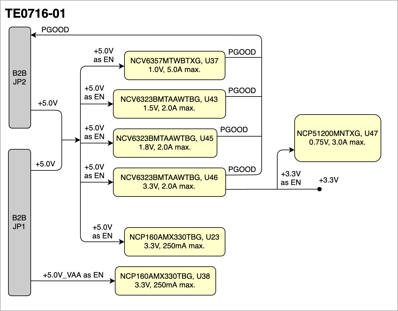 Image Added Image Added
| | Scroll Only |
|---|
image link to the generate DrawIO PNG file of this page. This is a workaround until scroll pdf export bug is fixed |
|
Voltage Monitor Circuit
| Scroll Title |
|---|
| anchor | Figure_PWR_VMC |
|---|
| title | Voltage Monitor Circuit |
|---|
|
| Scroll Ignore |
|---|
Create DrawIO object here: Attention if you copy from other page, objects are only linked. |
| Scroll Only |
|---|
image link to the generate DrawIO PNG file of this page. This is a workaround until scroll pdf export bug is fixed |
|
...
Technical Specifications
Absolute Maximum Ratings
| Scroll Title |
|---|
| anchor | Table_TS_AMR |
|---|
| title | PS absolute maximum ratings |
|---|
|
| Scroll Table Layout |
|---|
| orientation | portrait |
|---|
| sortDirection | ASC |
|---|
| repeatTableHeaders | default |
|---|
| style | |
|---|
| widths | |
|---|
| sortByColumn | 1 |
|---|
| sortEnabled | false |
|---|
| cellHighlighting | true |
|---|
|
| Symbols | Description | Min | Max | Unit | Reference |
|---|
| +5.0V | Main Supply voltage from the carrier board | -0.3 | 6.0 | V | NCV6357 Datasheet
NCV6323 Datasheet
NCP160 Datasheet | | +5.0V_VAA | Analog Supply voltage from the carrier board | -0.3 | 6.0 | V | NCP160 Datasheet | | MIO 500 | I/O input voltage for MIO bank 500 | -0.4 | 3.85 | V | Xilinx DS187 Datasheet | | MIO 501 | I/O input voltage for MIO bank 501 | -0.4 | 2.35 | V | Xilinx DS187 Datasheet | | PL HR | I/O input voltage for HR banks | -0.4 | 3.85 | V | Xilinx DS187 Datasheet | | ADCx_P/N | I/O input voltage for ADCs analog inputs | -0.3 | 3.63 | V | NCD98011 Datasheet |
|
| Scroll Title |
|---|
| anchor | Table_TS_AMR |
|---|
| title | PS absolute maximum ratings |
|---|
|
| Scroll Table Layout |
|---|
|
| orientation | portrait |
|---|
| sortDirection | ASC |
|---|
| repeatTableHeaders | default |
|---|
style | widths | | sortByColumn | 1 |
|---|
| sortEnabled | false |
|---|
| cellHighlighting | true |
|---|
| Symbols | Description | Min | Max | Unit |
|---|
V | V | V | V | V | V | V | V
Recommended Operating Conditions
...
| Scroll Title |
|---|
| anchor | Table_TS_ROC |
|---|
| title | Recommended operating conditions. |
|---|
|
| Scroll Table Layout |
|---|
| orientation | portrait |
|---|
| sortDirection | ASC |
|---|
| repeatTableHeaders | default |
|---|
| style | |
|---|
| widths | |
|---|
| sortByColumn | 1 |
|---|
| sortEnabled | false |
|---|
| cellHighlighting | true |
|---|
|
| Parameter | Min | Max | Units | Reference Document |
|---|
+5.0V Main Supply input voltage
from the carrier board |
|
| V | NCV6357 Datasheet NCV6323 Datasheet NCP160 Datasheet | +5.0V_VAA Analog Supply input voltage
from the carrier board |
|
| V | NCP160 Datasheet | | I/O input voltage for MIO bank 500 | -0.x |
| V | Xilinx DS187 Datasheet | | I/O input voltage for MIO bank 501 | -0.x |
| V | Xilinx DS187 Datasheet | | I/O input voltage for HR banks | -0.x |
| V | Xilinx DS187 Datasheet | | I/O input voltage for ADCs analog inputs | -0.x |
| V | NCD98011 Datasheet | See ???? datasheets. | V | See Xilinx ???? datasheet. | V | See Xilinx ???? datasheet. | V | See Xilinx ???? datasheet. | V | See Xilinx ???? datasheet. | V | See Xilinx ???? datasheet. | V | See Xilinx ???? datasheet. | °C | See Xilinx ???? datasheet. | °C | See Xilinx ???? datasheet. |
|
Physical Dimensions
Module size: 45 mm × 65 mm. Please download the assembly diagram for exact numbers.
Mating height with 61982 receptacle connectors: 5mm, 7mm, 13mm and 17mm stack heights.
PCB thickness: 1.65 mm.
...
| Scroll Title |
|---|
| anchor | Table_RH_HRH |
|---|
| title | Hardware Revision History |
|---|
|
| Scroll Table Layout |
|---|
| orientation | portrait |
|---|
| sortDirection | ASC |
|---|
| repeatTableHeaders | default |
|---|
| style | |
|---|
| widths | |
|---|
| sortByColumn | 1 |
|---|
| sortEnabled | false |
|---|
| cellHighlighting | true |
|---|
|
| Date | Revision | Changes | Documentation Link |
|---|
| 2020-10-25 | REV01 | Initial Release | REV01 |
|
Hardware revision number can be found on the PCB board together with the module model number separated by the dash.
...