...
| Scroll Title |
|---|
| anchor | Figure_OV_BD |
|---|
| title | TE0716-01 block diagram |
|---|
|
| Scroll Ignore |
|---|
| draw.io Diagram |
|---|
| border | false |
|---|
| |
|---|
| diagramName | DB-TE0716-01 |
|---|
| simpleViewer | false |
|---|
| width | |
|---|
| links | auto |
|---|
| tbstyle | hidden |
|---|
| diagramDisplayName | |
|---|
| lbox | true |
|---|
| diagramWidth | 641 |
|---|
| revision | 1819 |
|---|
|
|
| Scroll Only |
|---|
|
|
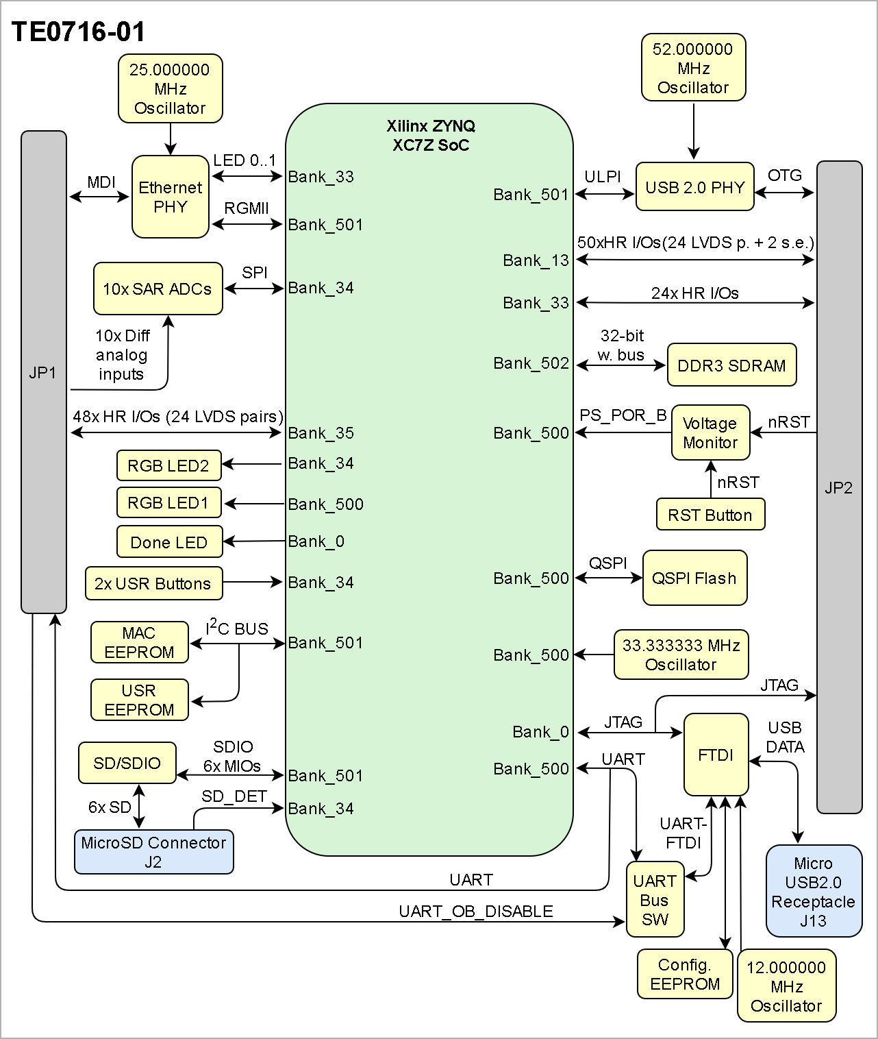
Main Components
...
| Scroll Title |
|---|
| anchor | Figure_PWR_PD |
|---|
| title | Power Distribution |
|---|
|
| Scroll Ignore |
|---|
| draw.io Diagram |
|---|
| border | false |
|---|
| |
|---|
| diagramName | PWR-PD-TE0716-01 |
|---|
| simpleViewer | false |
|---|
| width | |
|---|
| links | auto |
|---|
| tbstyle | hidden |
|---|
| diagramDisplayName | |
|---|
| lbox | true |
|---|
| diagramWidth | 643 |
|---|
| revision | 2 |
|---|
|
|
| Scroll Only |
|---|
|
|
Power-On Sequence
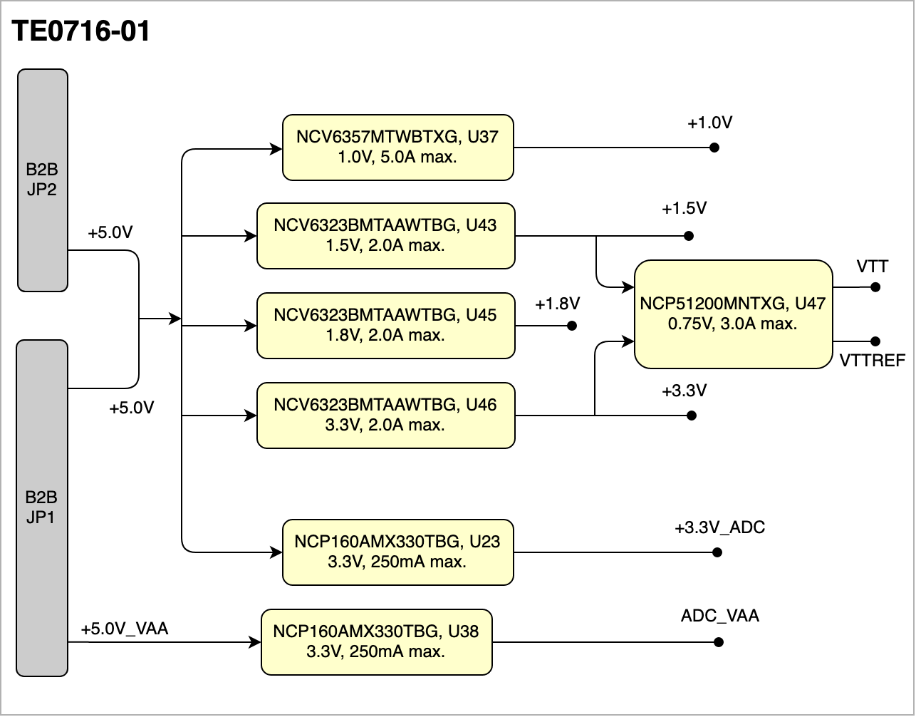
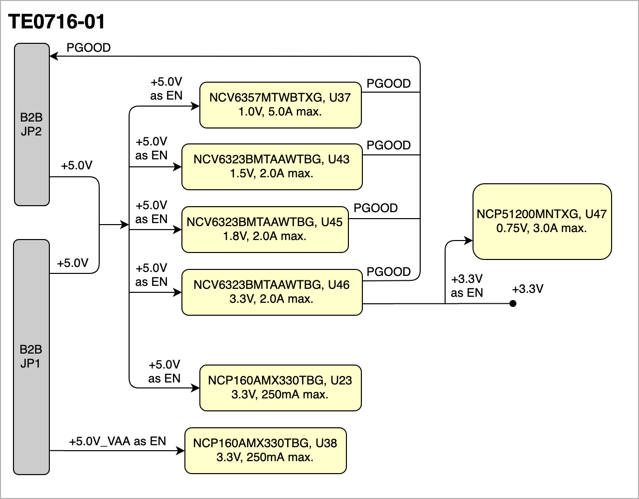
The TE0716 has only one common "PGOOD" signal (from U37, U43, U45 and U46), and there is no Enable for the board. You could control the startup of the board IC, by controlling the +5.0V and the +5.0V_VAA input signals only.
| Scroll Title |
|---|
| anchor | Figure_PWR_PS |
|---|
| title | Power Sequency |
|---|
|
| Scroll Ignore |
|---|
| draw.io Diagram |
|---|
| border | true |
|---|
| |
|---|
| diagramName | PWR-PS-TE0716-01 |
|---|
| simpleViewer | false |
|---|
| width | |
|---|
| links | auto |
|---|
| tbstyle | top |
|---|
| lbox | true |
|---|
| diagramWidth | 641 |
|---|
| revision | 3 |
|---|
|
|
| Scroll Only |
|---|
|
|
Voltage Monitor Circuit
The TE0716 has also a Voltage Monitor IC. It keeps nRST signal low if the FPGA core voltage (+1.0V) drops under 0.84V or the 3.3V power supply drops to 2.94V or less.
Power Good signal is unique and comes from the power supplies IC U37, U43, U45 and U46, as you can see in the previous section "Power-On Sequence", and also could make nRST to remain low until PGOOD is high.
See also "Reset process." section in "Configuration Signals" for additional information.
| Scroll Title |
|---|
| anchor | Figure_PWR_VMC |
|---|
| title | Voltage Monitor Circuit |
|---|
|
| Scroll Ignore |
|---|
| draw.io Diagram |
|---|
| border | false |
|---|
| |
|---|
| diagramName | PWR-PM-TE0716-01 |
|---|
| simpleViewer | false |
|---|
| width | |
|---|
| links | auto |
|---|
| tbstyle | hidden |
|---|
| diagramDisplayName | |
|---|
| lbox | true |
|---|
| diagramWidth | 642641 |
|---|
| revision | 12 |
|---|
|
|
| Scroll Only |
|---|
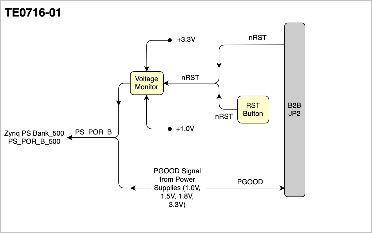 Image Added Image Added
|
|
Power Rails
| Scroll Title |
|---|
| anchor | Table_PWR_PR |
|---|
| title | Module power rails. |
|---|
|
| Scroll Table Layout |
|---|
| orientation | portrait |
|---|
| sortDirection | ASC |
|---|
| repeatTableHeaders | default |
|---|
| style | |
|---|
| widths | |
|---|
| sortByColumn | 1 |
|---|
| sortEnabled | false |
|---|
| cellHighlighting | true |
|---|
|
| Power Rail Name | B2B Connector JP1 Pin | B2B Connector JP2 Pin | Direction | Notes |
|---|
| +5.0V | 1, 2, 3 | 1, 2, 3 | Input | Main Supply voltage from the carrier board | | +5.0V_VAA | 43, 44 | - | Input | Analog Supply voltage from the carrier board | | +3.3V (VREF_JTAG) | - | 5 | Output | JTAG reference voltage. |
|
...