Page History
| Children Display |
|---|
...
Download PDF version of this document.
| Scroll pdf ignore | |
|---|---|
Table of Contents
|
Overview
| Scroll Only (inline) |
|---|
Refer to https://shop.trenz-electronic.de/de/Download/?path=Trenz_Electronic/TE0713 for downloadable version of this manual and the rest of available documentation.
|
Block Diagram
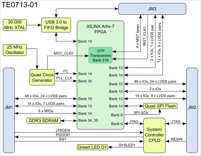
Main Components
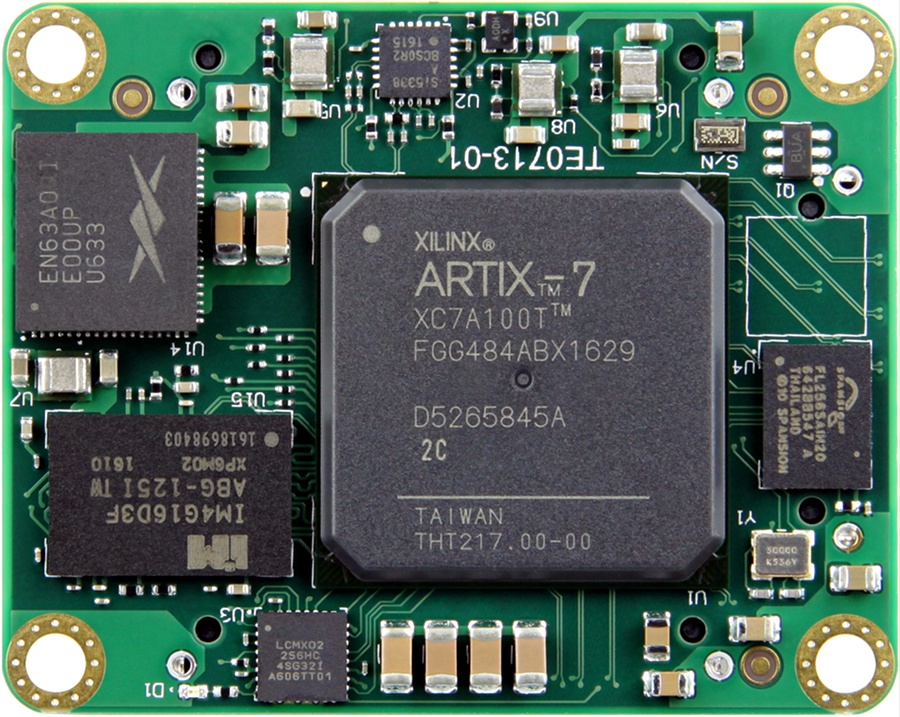
- Xilinx Artix-7 XC7A series FPGA, U1
- ...
- ...
- System Controller CPLD, Lattice Semiconductor MachXO2-256HC, U3
- ...
Key Features
- Xilinx Artix-7 (15T to 200T) SoM (System on Module)
- Both industrial and commercial temperature ranges available
- Rugged for high shock and high vibration resistance
- 1 GByte DDR3 32-bit SDRAM
- 32 MByte QSPI Flash memory (with XiP support)
- Programmable clock generator
- GTP transceiver clock (default 125 MHz)
- Fabric clock (default 200 MHz)
- GTP transceiver clock (default 125 MHz)
- Plug-on module with 2 × 100-pin and 1 × 60-pin high-speed hermaphroditic strips
- 142 FPGA I/Os (71 differential pairs) available on board-to-board connectors
- 4 GTP (multi gigabit transceiver) lanes
- External clock input for GTP transceivers via B2B connector
- On-board high-efficiency DC-DC converters
- System management and power sequencing
- eFUSE bit-stream encryption
- AES bit-stream encryption
- User configurable LED
Evenly-spread supply pins for good signal integrity
Additional assembly options are available for cost or performance optimization upon request.
Initial Delivery State
...
Programmable unit
...
Content
...
Notes
...
SPI Flash main array
...
Signals, Interfaces and Pins
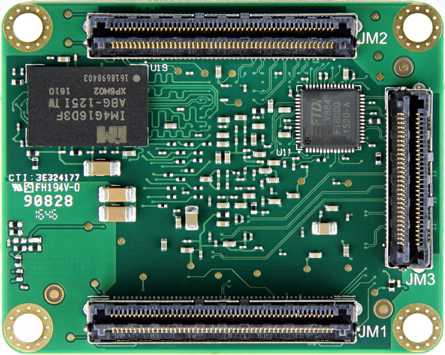
Board to Board (B2B) I/Os
FPGA banks and I/O signals connected to the B2B connectors:
...
JTAG Interface
JTAG access to the Xilinx Artix-7 FPGA and System Controller CPLD devices is provided through B2B connector JM2.
...
JTAG Signal
...
B2B Pin
...
JTAGEN pin in B2B connector JM1 is used to select JTAG access for FPGA or SC CPLD:
...
System Controller I/O Pins
Special purpose pins are connected to System Controller CPLD and have following default configuration:
...
LEDs
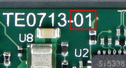
The TE0713-01 module has one LED which is connected to the System Controller CPLD. Once FPGA configuration has completed, it can be used by the user's design.
...
Clocking
Si5338 programmable clock generator chip is used to generate clocks with 25 MHz oscillator as input connected to the pin IN3. There is a I2C bus connected between the FPGA bank 14 (master) and clock generator chip (slave) which can be used to program output frequencies. See the reference design for more information.
On-board Peripherals
32 MByte Quad SPI Flash Memory
On-board QSPI flash memory S25FL256S (U14) is used to store initial FPGA configuration. Besides FPGA configuration, remaining free flash memory can be used for user application and data storage. All four SPI data lines are connected to the FPGA allowing x1, x2 or x4 data bus widths. Maximum data rate depends on the selected bus width and clock frequency used.
| Note |
|---|
SPI Flash QE (Quad Enable) bit must be set to high or FPGA is unable to load its configuration from flash during power-on. By default this bit is set to high at the manufacturing plant. |
System Controller CPLD
System Controller CPLD (Lattice MachXO2-256HC, U3) is used to control FPGA configuration process. The FPGA is held in reset (by driving the PROG_B signal low) until all power supplies have stabilized.
By driving signal RESIN to low you can reset the FPGA. This signal can be driven from the user’s baseboard PCB via the B2B connector JM2 pin 18.
Input EN1 is also gated to FPGA reset, should be open or pulled up for normal operation. By driving EN1 low, on-board DC-DC converters will be not turned off.
User can create their own System Controller design using Lattice Diamond software. Once created it can be programmed into CPLD via JTAG interface.
DDR3 SDRAM
The TE0713-01 SoM has two 4 Gbit volatile DDR3 SDRAM ICs (U15 and U19) for storing user application code and data.
- Part number: IM4G16D3FABG-125I
- Supply voltage: 1.35V
- Organization: 32M words x 16 bits x 8 banks
- Memory speed: limited by Xilinx Artix-7 speed grade and MIG
Configuration of the DDR3 memory controller in the FPGA should be done using the MIG tool in the Xilinx Vivado Design Suite IP catalog.
USB 3.0 to FIFO Bridge
...
Power and Power-On Sequence
Power Supply
Single 3.3V power supply (for both VIN and 3.3VIN power rails) with minimum current capability of 3A for system startup is recommended.
Power Consumption
Typical module power consumption is between 2-3W. Exact power consumption is to be determined.
TE0713-01 module can also be powered by split 5V/3.3V power sources if preferred. In such case apply 5V to B2B connectors VIN pins and 3.3V to 3.3VIN pins, although lowest power consumption is achieved when powering the module from single 3.3V supply. When using split 5V/3.3V supplies the power consumption (and heat dissipation) will rise due to the DC-DC converter efficiency (it decreases when VIN/VOUT ratio rises).
Power-On Sequence
For the highest efficiency of the on-board DC-DC regulators, it is recommended to use same 3.3V power source for both VIN and 3.3VIN power rails. Although VIN and 3.3VIN can be powered up in any order, it is recommended to power them up simultaneously.
It is important that all baseboard I/Os are 3-stated at power-on until System Controller sets PGOOD signal high (B2B connector JM1, pin 30), or 3.3V is present on B2B connector JM2 pins 10 and 12, meaning that all on-module voltages have become stable and module is properly powered up.
See Xilinx datasheet DS181 - "Artix-7 FPGAs Data Sheet: DC and AC Switching Characteristics" for additional information. User should also check related baseboard documentation when choosing baseboard design for TE0713 module.
Power Rails
...
Power Rail Name
...
B2B Connector JM1 Pin
...
B2B Connector JM2 Pin
...
Direction
...
VIN
...
1.8V
...
Module internal 1.8V level. Maximum 300mA available.
...
High-Range bank supply voltage (from the baseboard).
...
Board to Board Connectors
...
Technical Specifications
Absolute Maximum Ratings
...
Parameter
...
Units
...
Reference Document
...
VIN supply voltage
...
V
...
Storage temperature (ambient)
...
-55
...
100
...
°C
...
Recommended Operating Conditions
...
| Note |
|---|
| Assembly variants for higher storage temperature range are available on request. |
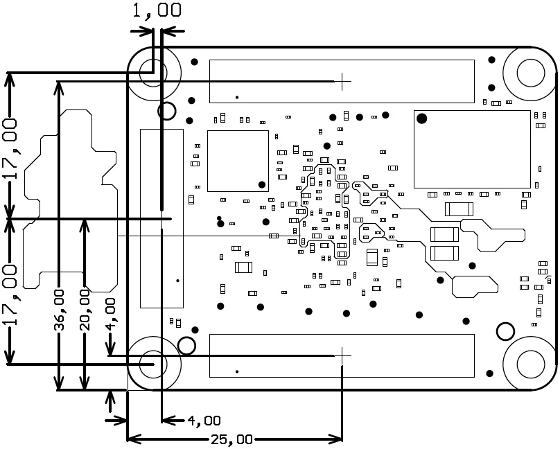
Physical Dimensions
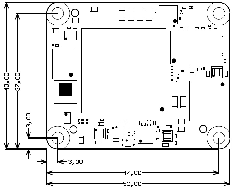
- Module size: 50 mm × 40 mm. Please download the assembly diagram for exact numbers.
- Mating height with standard connectors: 8mm
- PCB thickness: 1.6mm
- Highest part on PCB: approx. 2.5mm. Please download the step model for exact numbers.
All dimensions are shown in millimeters.
Operating Temperature Ranges
Commercial grade: 0°C to +70°C.
Industrial grade: -40°C to +85°C.
Operating temperature range depends also on customer design and cooling solution. Please contact us for options.
Weight
21 g Plain module.
8.8 g Set of nuts and bolts.
Revision History
Hardware Revision History
...
Notes
...
01
...
First production revision
...
Document Change History
...
Date
...
Revision
...
Contributors
...
Description
...
Disclaimer
Include Page
Overview
Content Tools