Page History
| Scroll Ignore |
|---|
| Scroll pdf ignore | |
|---|---|
Table of Contents
|
Overview
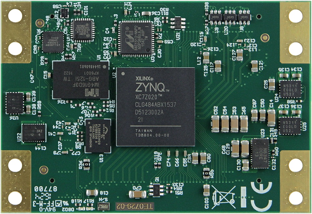
The Trenz Electronic TE0729 is an industrial-grade SoM (System on Module) based on AMD Zynq-7000 SoC (XC7Z020).
| Scroll Only (inline) |
|---|
...
Refer to trenz.org/te0729-info for online version of this manual and |
...
additional technical |
...
documentation |
...
of |
...
the |
...
product. |
...
Key Features
The Trenz Electronic TE0729 is an industrial-grade SoM (System on Module) based on Xilinx Zynq-7000 SoC (XC7Z020).
Key Features
- Industrial-grade Xilinx AMD Zynq-7000 (XC7Z020) SoM
- Dual-core ARM Cortex-A9 MPCore™ with CoreSight™
- 136 x FPGA I/Os (58 LVDS pairs possible)
- 8 x PS MIO pins
- 16-bit wide 512 MByte DDR3 SDRAM
- 32 MByte QSPI Flash memory
- 4 GByte eMMC Flash memory
- 1 x 10/100/1000 Mbps Ethernet transceiver PHY
- 2 x 10/100 Mbps Ethernet transceiver PHY'sPHYs
- 3 x MAC address EEPROM'sEEPROMs
- Hi-speed USB 2.0 ULPI transceiver with full OTG support
- Plug-on module with two 120-pin connectors
- Evenly - spread supply pins for good signal integrity
- On-board high-efficiency DC-DC converters
- 4.0 6 A x 1.0 V power rail
- 1.5 3 A x 1.5 V power rail1.
- 5 3 A x 1.8 V power rail
- 1.5 3 A x 2.5 V power rail
- System management
- eFUSE bit-stream encryption
- AES bit-stream bitstream encryption
- Temperature compensated RTC (real-time clock)
- User LED
- Rugged for shock and high vibration
...
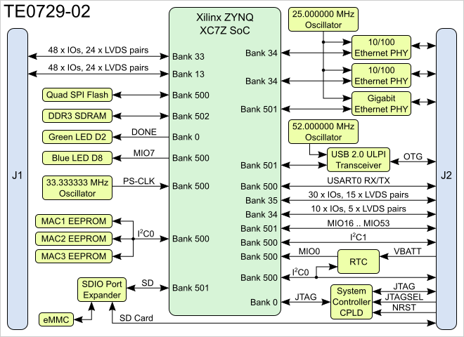
Block Diagram
Main Components
Initial Delivery State
...
24AA025E48 EEPROM's
...
User content not programmed
...
SPI Flash OTP Area
...
Empty, not programmed
...
Except serial number programmed by flash vendor
...
SPI Flash Quad Enable bit
...
Programmed
...
SPI Flash main array
...
demo design
...
eFUSE USER
...
Not programmed
...
eFUSE Security
...
Not programmed
...
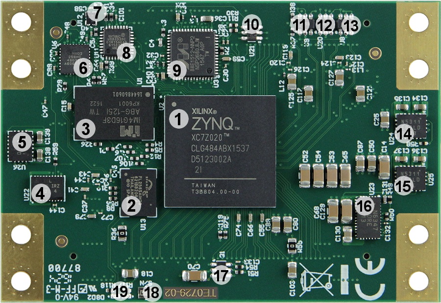
- AMD Zynq-7000 all programmable SoC, U2
- 32 MByte quad SPI Flash memory, U13
- 4 Gbit DDR3/L SDRAM, U1
- Low-power RTC with battery backed SRAM, U22
- 3 A PowerSoC DC-DC converter (1.5V), U26
- System Controller CPLD, U6
- Low-power programmable oscillator @ 52.000000 MHz (OTG-RCLK), U12
- Hi-speed USB 2.0 ULPI transceiver, U11
- Gigabit Ethernet (GbE) transceiver, U3
- Ultra-low supply-current voltage monitor, U21
- 2K I2C serial EEPROM with EUI-48™ node identity, U9
- 2K I2C serial EEPROM with EUI-48™ node identity, U20
- 2K I2C serial EEPROM with EUI-48™ node identity, U8
- 3 A PowerSoC DC-DC converter (2.5V), U24
- 3 A PowerSoC DC-DC converter (1.8V), U25
- 6 A PowerSoC DC-DC converter (1.0V), U23
- 3 A PFET load switch with configurable slew rate (3.3V), Q1 (position changed for REV03)
- Serial number (traceability) pad (position on bottom for REV03).
- Green LED D2 and red LED D8
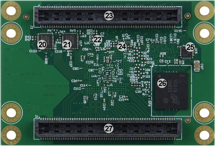
- 10Base-T/100Base-TX Ethernet PHY, U19
- 10Base-T/100Base-TX Ethernet PHY, U17
- Low-power programmable oscillator @ 25.000000 MHz (ETH_CLKIN), U10
- 120-pin double-row REF-189019-02 B2B connector, J2
- Low-power programmable oscillator @ 33.333333 MHz (PS-CLK), U14
- SDIO port expander with voltage-level translation, U15
- eMMC NAND Flash, U5
- 120-pin double-row REF-189019-02 B2B connector, J1
Initial Delivery State
| Storage device name | Content | Notes |
|---|---|---|
24AA025E48 EEPROMs | User content not programmed | Valid MAC address from manufacturer |
| eMMC Flash-Memory | Empty, not programmed | Except serial number programmed by flash vendor |
SPI Flash OTP Area | Empty, not programmed | Except serial number programmed by flash vendor |
SPI Flash Quad Enable bit | Programmed | |
SPI Flash main array | Demo design | |
eFUSE USER | Not programmed | |
eFUSE Security | Not programmed |
Signals, Interfaces and Pins
Board to Board (B2B) I/Os
| Bank | Type | B2B | IO count | IO Voltage | Notes |
|---|---|---|---|---|---|
| 500 | MIO | J2-87 J2-88 | 2 | 3.3 V | MIO0, MIO9 |
| 500 | MIO | J2-93 J2-95 J2-94 J2-96 | 4 | 3.3 V | Configured as I2C1 and USART0 by default, Configurable as GPIO by user |
| 13 | HR | J1 | 48 | User | |
| 33 | HR | J1 | 48 | User | |
| 35 | HR | J2 | 30 | 3.3 V | |
| 34 | GPIO | J2 | 10 | 2.5 V | Configured as DISP_RX by default, Configurable as GPIO by user |
For detailed information about the pin out, please refer to the Master Pin-out table.
JTAG Interface
JTAG access to the AMD Zynq-7000 device is provided through B2B connector J2.
| Signal | B2B Pin |
|---|---|
| TCK | J2-119 |
| TDI | J2-115 |
| TDO | J2-117 |
| TMS | J2-113 |
| Note |
|---|
JTAGSEL pin 111 of B2B connector J2 should be kept low or grounded for normal operation. |
System Controller I/O Pins
Special purpose pins used by TE0729:
| Name | Note |
|---|---|
| NRST | Reset-Signal from Watchdog, available at B2B J2-89 |
| NRST_IN | External Reset, available at B2B J2-91 |
For details see: TE0729 CPLD
On-board LEDs
There are 3 LED's on TE0729:
| LED | Color | Connected to | Notes |
|---|---|---|---|
| D1 | red | System Controller | Global Status LED |
| D2 | green | DONE | Inverted DONE, ON when FPGA not configured |
| D8 | red | MIO7 | OFF when PS7 not booted and not controlling MIO7 by software, else user controlled |
| Note |
|---|
LED D2 is connected to the FPGA Done pin and will go off as soon as PL is configured. This LED will not operate if the System Controller can not power on the 3.3V output rail that also powers the 3.3V circuitry on the module. |
Clocking
| Clock | Frequency | IC | FPGA | Notes |
|---|---|---|---|---|
| PS-CLK | 33.333333 MHz | U14 | PS_CLK | PS subsystem main clock |
| ETH_CLKIN | 25.000000 MHz | U10 | - | Ethernet PHYs reference clock |
| 52.000000 MHz | U12 | - | USB PHY reference clock |
Default MIO mapping
| MIO | Configured as | B2B | Notes |
|---|---|---|---|
| 0 | GPIO | J2-87 | B2B |
| 1 | QSPI0 | - | SPI Flash-CS |
| 2 | QSPI0 | - | SPI Flash-DQ0 |
| 3 | QSPI0 | - | SPI Flash-DQ1 |
| 4 | QSPI0 | - | SPI Flash-DQ2 |
| 5 | QSPI0 | - | SPI Flash-DQ3 |
| 6 | QSPI0 | - | SPI Flash-SCK |
| 7 | GPIO | - | Red LED D8 |
| 8 | - | - | QSPI feedback clock |
| 9 | GPIO | J2-88 | B2B |
| 10 | I2C0 SDA | J2-90 | B2B |
| 11 | I2C0 SCL | J2-92 | B2B |
| 12 | I2C1 SDA | J2-93 | B2B (SDA on-board I2C, also configurable as GPIO by user) |
| 13 | I2C1 SCL | J2-95 | B2B (SCL on-board I2C, also configurable as GPIO by user) |
| 14 | USART0 RX | J2-94 | B2B (RX on-board UART, also configurable as GPIO by user) |
| 15 | USART0 TX | J2-96 | B2B (TX on-board UART, also configurable as GPIO by user) |
| 16..27 | ETH0 | Ethernet RGMII PHY | |
| 28..39 | USB0 | USB ULPI PHY | |
| 40 | SDIO0 | J2-100 | |
| 41 | SDIO0 | J2-102 | |
| 42 | SDIO0 | J2-104 | |
| 43 | SDIO0 | J2-106 | |
| 44 | SDIO0 | J2-108 | |
| 45 | SDIO0 | J2-110 | |
| 46 | GPIO | - | RTC Interrupt |
| 47 | - | - | - |
| 48 | GPIO | SEL_SD | SD Card multiplexer control |
| 49 | GPIO | - | USB Reset |
| 50 | GPIO | - | ETH0 Interrupt |
| 51 | GPIO | - | ETH0 Reset |
| 52 | ETH0 | - | MDC |
53 | ETH0 | - | MDIO |
Boot Modes
TE0729 supports primary boot from
- JTAG
- SPI Flash
- SD Card
Boot from on-board eMMC is also supported as secondary
Signals, Interfaces and Pins
Board to Board (B2B) I/Os
...
J2-87
J2-88
...
J2-93
J2-95
J2-94
J2-96
...
Configured as I2C1 and USART0 by default,
Configurable as GPIO by user
...
Configured as DISP_RX by default,
Configurable as GPIO by user
For detailed information about the pin out, please refer to the Master Pin-out table.
JTAG Interface
JTAG access to the Xilinx Zynq-7000 device is provided through connector J2.
...
| Note |
|---|
JTAGSEL pin in J2 should be kept low or grounded for normal operation. |
System Controller I/O Pins
Special purpose pins used by TE0729:
...
On-board LEDs
There are 3 LED's on TE0729:
...
| Note |
|---|
LED D2 is connected to the FPGA Done pin and will go off as soon as PL is configured. This LED will not operate if the System Controller can not power on the 3.3V output rail that also powers the 3.3V circuitry on the module. |
Clocking
...
Default MIO mapping
...
53
...
Boot Modes
TE0729 supports primary boot from
- JTAG
- SPI Flash
- SD Card
Boot from on-board eMMC is also supported as secondary boot (FSBL must be loaded from SPI Flash).
...
| Peripheral | IC | Designator | PS | MIO | Notes | |||
|---|---|---|---|---|---|---|---|---|
| EEPROM I2C | 24AA025E48T-I/OT | U8 | I2C0 | MIO10, MIO11 | MAC Address | |||
| EEPROM I2C | 24AA025E48T-I/OT | U9 | I2C0 | MIO10, MIO11 | MAC Address | |||
| EEPROM I2C | 24AA025E48T-I/OT | U20 | I2C0 | MIO10, MIO11 | MAC Address | |||
| RTC | ISL12020MIRZ | U22 | I2C0 | MIO10, MIO11 | Temperature compensated real time clock | |||
| RTC Interrupt | ISL12020MIRZ | U22 | GPIO | MIO46 | Real Time Clock Interrupt | |||
| SPI Flash | S25FL256SAGBHI20 | U13 | QSPI0 | MIO1..MIO6 | ||||
| Ethernet0 10/100/1000 Mbps PHY | 88E1512-A0-NNP2I000 | U3 | ETH0 | MIO16...MIO27 | ||||
| Ethernet0 10/100/1000 Mbps PHY Reset | GPIO | GPIO | MIO51 | |||||
| Ethernet1 10/100 Mbps PHY | KSZ8081MLXCA | U17 | - | (EMIO) | ||||
| Ethernet1 10/100 Mbps PHY Reset | - | (EMIO) | ||||||
| Ethernet2 10/100 Mbps PHY | KSZ8081MLXCA | U19 | - | (EMIO) | ||||
| Ethernet2 10/100 Mbps PHY Reset | - | (EMIO) | ||||||
| USB | USB3320C-EZK | U11 | USB0 | MIO28...MIO39 | ||||
| USB Reset | GPIO | MIO49 | ||||||
| eMMC eMMC (embedded eMMC) | MTFC4GMVEA-4M IT | U5 | SDIO0 | MIO40...MIO45 |
I2C Interface
The on-board I2C components are connected to MIO10 and MIO11 and configured as I2C0 by default.
...
| Device | I2C-Address | Notes | |
|---|---|---|---|
| EEPROM for MAC1 | 0x50 | ||
| EEPROM for MAC2 | 0x51 | ||
| EEPROM for MAC3 | 0x52 | ||
| RTC | 0x6F | ||
| Battery backed RAM | 0x57 | Integrated in RTC |
...
| PHY PIN | ZYNQ PS | Notes |
|---|---|---|
| MDC/MDIO | MIO52, MIO53 | - |
| LED0 | - | pin J2-57 on B2B connector |
| LED1 | - | pin J2-59 on B2B connector |
| LED2/Interrupt | MIO46 | - |
| CONFIG | - | Connected to GND, PHY Address 0 |
| RESETn | MIO51 | - |
| RGMII | MIO16..MIO27 | - |
| SGMII | - | B2B J2 |
| MDI | - | B2B J2 |
The TE0729 SoM is also equipped is also equipped with two additional Microchip KSZ8081MLXCA Ethernet PHY's (IC's U17 and U19) to provide further 10/100 Mbps Ethernet interfaces with the identifiers Ethernet1 and Ethernet2. The reference clock input of both PHYs is supplied from the same 25MHz 25 MHz oscillator (U10), which also provides Ethernet0 Gigabit PHY with a reference clock signal.
Ethernet1 PHY connection to B2B-connectors:
| PHY PIN | B2B | notesNotes |
|---|---|---|
| ETH1_RX_P | J2-26 | - |
| ETH1_RX_N | J2-28 | - |
| ETH1_TX_P | J2-20 | - |
| ETH1_TX_N | J2-22 | - |
| ETH1_LED0 | J2-34 | Status LED |
| ETH1_LED1 | J2-32 | Transmission LED |
Ethernet2 PHY connection to B2B-connectors:
| PHY PIN | B2B | notesNotes |
|---|---|---|
| ETH2_RX_P | J2-2 | - |
| ETH2_RX_N | J2-4 | - |
| ETH2_TX_P | J2-8 | - |
| ETH2_TX_N | J2-10 | - |
| ETH2_LED0 | J2-16 | Status LED |
| ETH2_LED1 | J2-14 | Transmission LED |
All other pins of the PHYs are connected to Bank34 of Zynq, see schematic for further details.
USB Interface
The USB PHY Microchip USB3320 from Microchip is used on the TE0729. The ULPI interface is connected is connected via ULPI interface to the Zynq PS USB0. The I/O Voltage voltage level is fixed at 1.8V .The and PHY reference clock input of the PHY is supplied from an the on-board 52MHz 52.000000 MHz oscillator (U12).
PHY connection:
| PHY Pin | Zynq Pin | B2B Name | Notes |
|---|---|---|---|
| ULPI | MIO28..39 | - | Zynq USB0 MIO pins are connected to the PHY |
| REFCLK | - | - | 52MHz from on board oscillator (U12) |
| REFSEL[0..2] | - | - | 000 All three connected to the GND, select 52MHz reference Clockselects 52.000000 MHz as reference clock |
| RESETB | MIO49 | - | Active-low reset |
| CLKOUT | MIO36 | - | Connected to 1.8V, selects reference clock operation mode |
| DP,DM | - | OTG_D_P, OTG_D_N | USB Data data lines |
| CPEN | - | VBUS_V_EN | External USB power switch active-high enable signal |
| VBUS | - | USB_VBUS | Connect Connected to the USB-VBUS via a series resistor. Check reference schematic |
| ID | - | OTG_ID | For an A-Device connect connected to the ground, for a B-Device left floating |
...
Battery backed registers are accessed at I2C slave address 0x57. General purpose RAM is accessed at I2C slave address 0x6F. This RTC IC is supported in by the Linux OS, so it can be used as hwclock device.
MAC-Address
...
EEPROMs
TE0729 module has three Microchip 24AA025E48 EEPROMs
...
Three Microchip 24AA025E48 EEPROM's (U8, U9 , and U20) are used on the TE0729. They which contain globally unique 48-bit node addresses, that are compatible with EUI-48(TM) and EUI-64(TM). The devices compatible 48-bit node (MAC) addresses. These EEPROMs are organized as two blocks of 128 x 8-bit memory. One of those the blocks stores the 48-bit node address and is write protected, the other block is available for application use. It is accessible through the I2C EEPROMs are accessible using I2C slave address 0x50 for MAC-Address1 (U8), 0x51 for MAC-Address2 (U9), 0x52 for MAC-Address3 (U20).
...
TE0729 has support for hardware watchdog function. With standard variant, By default the watchdog is disabled at power up. Please contact Trenz Electronic for details how to enable watchdog function.
...
For startup, a power supply with minimum current capability of 3A 3 A is recommended.
VIN and 3.3VIN can be connected to the same source (3.3 V).
...
Supply Voltage | Voltage Range | Notes |
|---|---|---|
VIN | 3.3 V to 5.5 V |
|
| VIN 3.3V | 3.3 V |
|
Bank Voltages
| Bank | Voltage | Max. Value | Notes |
|---|---|---|---|
| 501 | 1,.8 V | - | ETH0 / USB0 / SDIO0 |
| 500 | 3,.3 V | - | SPI / I2C / UART |
| 502 | 1,.5 V | - | DDR3-RAM |
| 13 | user | 3,.3 V | connected to 3,.3V by default by 0-Ohm-Resistor R36 |
| 33 | user | 3,.3 V | connected to 3,.3V by default by 0-Ohm-Resistor R55 |
| 34 | 2,.5 V | - | ETH / DISP |
| 35 | 3,.3 V | - | GPIO |
Power-up sequence at start-up
...
Pay attention to the voltage level of the I/O-signals, which must not be higher than VCCIO + 0.4V.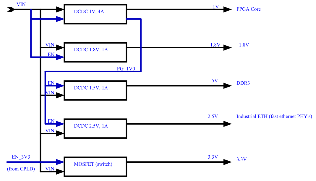
| Warning |
|---|
| Power-up sequencing changed for REV03. Please, take a look at schematics (Power Overview) for REV03 power-up sequencing. |
Board to Board Connectors
The TE0729 module has two 120-pin double-row REF-189019-02 connectors on the bottom side which are compatible with Samtec BTEBSE-060-01-L-D-A connectors. Mating connectors on the baseboard are REF-189019-01, which are compatible with Samtec BSEBTE-060-01-L-D-A connectors.
Connector Specifications
Insulator material: Liquid crystal polymer
Stacking height: 5 mm
Contact material: Phosphor-bronze
Plating: Au or Sn over 50 μ" (1.27 μm) Ni
Current rating: 2 A per pin (1 pin powered per row)
Operating temperature range: -55 °C to +125 °C
Voltage rating: 225 VAC with 5 mm stack height
Max cycles: 100
RoHS compliant: Yes
Technical Specification
Absolute Maximum Ratings
...
Vin supply voltage
...
-0.1
...
3.75
...
V
...
Voltage on Module JTAG pins
...
-0.4
...
V
...
Storage Temperature
...
-40
...
+85
...
C
...
| Note |
|---|
| Assembly variants for higher storage temperature range on request |
| Note |
|---|
| Please check Xilinx Datasheet for complete list of Absolute maximum and recommended operating ratings for the Zynq device (DS181 Artix or DS182 Kintex). |
Recommended Operating Conditions
...
Order | REF Number | Samtec Number | Type | Mated Height | Data sheet | Comment |
|---|---|---|---|---|---|---|
| - | REF-189019-02 | BTE-060-01-L-D-A-K-TR | Module connector | 5 mm | http://suddendocs.samtec.com/catalog_english/bte.pdf | Standard connector used on module |
| 26663 | REF-189019-01 | BSE-060-01-L-D-A-TR | Baseboard connector | 5 mm | http://suddendocs.samtec.com/catalog_english/bse.pdf | Standard connector used on board |
| Connector Specifications | Value |
|---|---|
| Insulator material | Liquid crystal polymer |
| Stacking height | 5 mm |
| Contact material | Phosphor-bronze |
| Plating | Au or Sn over 50 μ" (1.27 μm) Ni |
| Current rating | 2 A per pin (1 pin powered per row) |
| Operating temperature range | -55 °C to +125 °C |
| Voltage rating | 225 VAC with 5 mm stack height |
| Max cycles | 100 |
| RoHS compliant | Yes |
Technical Specification
Absolute Maximum Ratings
| Parameter | Min | Max | Units | Notes |
|---|---|---|---|---|
VIN supply voltage | -0.1 | 3.75 | V | |
| VBAT supply voltage | -0.3 | 6.0 | V | |
| PL I/O bank supply voltage for HR I/O banks (VCCO) | -0.5 | 3.6 | V | |
| I/O input voltage for HR I/O banks | -0.55 | VCCO_X+0.55 | V | |
Voltage on module JTAG pins | -0.4 | VCCO_0+0.55 | V | VCCO_0 is 3.3V nominal |
Storage temperature | -40 | +85 | C | |
| Storage temperature without the ISL12020MIRZ | -55 | +100 | C |
| Note |
|---|
| Assembly variants for higher storage temperature range on request |
| Note |
|---|
| Please check AMD Datasheet for complete list of Absolute maximum and recommended operating ratings for the Zynq device (DS181 Artix or DS182 Kintex). |
Recommended Operating Conditions
| Parameter | Min | Max | Units | Notes | Reference document |
|---|---|---|---|---|---|
| VIN supply voltage | 3.135 | 3.465 | V | ||
| VBAT supply voltage | 1.8 | 5.5 | V | ||
| PL I/O bank supply voltage for HR I/O banks (VCCO) | 1.14 | 3.465 | V | AMD document DS191 | |
| I/O input voltage for HR I/O banks | (*) | (*) | V | (*) Check datasheet | AMD document DS191 and DS187 |
| Voltage on module JTAG pins | 3.135 | 3.465 | V | VCCO_0 is 3.3 V nominal |
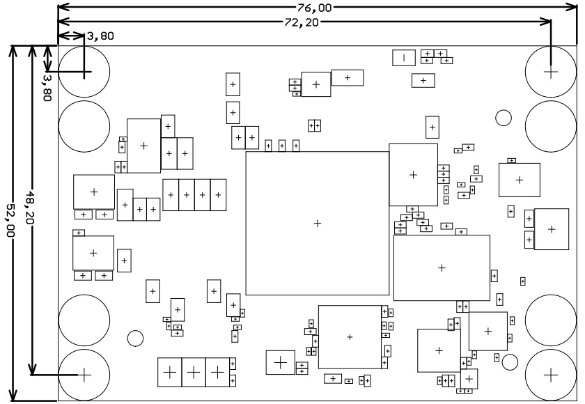
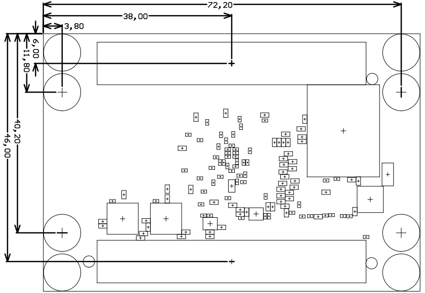
Physical Dimensions
Please download the assembly diagram for exact values.
Module size: 76 mm × 52 mm.
Mating height with standard connectors: 5 mm.
PCB thickness: 2 mm.
All dimensions are shown in millimeters.
Operating Temperature Ranges
Commercial grade modules
All parts are at least commercial temperature range of 0°C to +70°C.
Industrial grade modules
All parts are at least industrial temperature range of -40°C to +85°C.
The module operating temperature range depends on customer design and cooling solution. Please contact us for options.
Weight
Weight | Part |
|---|---|
21.6 g | Plain module |
Revision History
Hardware Revision History
| Date | Revision | Changes |
|---|---|---|
| 2023-12-01 | 03 |
|
| 2016-05-02 | 02 | First production release |
| - | 01 | Prototypes |
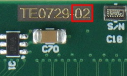
Hardware revision number is written on the PCB board together with the module model number separated by the dash.
Document Change History
| Date | Revision | Contributors | Description | ||||||||||||||||||||||||||
|---|---|---|---|---|---|---|---|---|---|---|---|---|---|---|---|---|---|---|---|---|---|---|---|---|---|---|---|---|---|
|
|
|
| ||||||||||||||||||||||||||
2022-07-13 | v.30 | Martin Rohrmüller |
| ||||||||||||||||||||||||||
2018-08-29 | v.29 | John Hartfiel |
| ||||||||||||||||||||||||||
| 2017-11-06 | v.28 | Ali Naseri |
| ||||||||||||||||||||||||||
| 2017-06-18 | v.22 | Jan Kumann |
| ||||||||||||||||||||||||||
| 2017-06-07 | v.21 | Jan Kumann |
| ||||||||||||||||||||||||||
2017-05-22 | v |
Physical Dimensions
Please download the assembly diagram for exact values.
Module size: 76 mm × 52 mm.
Mating height with standard connectors: 4,25 mm.
PCB thickness: 2 mm.
All dimensions are shown in millimeters.
Operating Temperature Ranges
Commercial grade modules
All parts are at least commercial temperature range of 0°C to +70°C.
Industrial grade modules
All parts are at least industrial temperature range of -40°C to +85°C.
The module operating temperature range depends on customer design and cooling solution. Please contact us for options.
Weight
...
Weight
...
Part
...
21,6 g
...
Plain module
Revision History
Hardware Revision History
...
01
...
Prototypes
Hardware revision number is written on the PCB board together with the module model number separated by the dash.
Document Change History
| Date | Revision | Contributors | Description | |||
|---|---|---|---|---|---|---|
| 2017-06-07 | Jan Kumann | Minor formatting | 2017-05-22 | V.12 | Jan Kumann |
|
| 2017-03-24 | Vv.11 | John Hartfiel |
| |||
| 2016-06-14 | Vv.10 | Ali Naseri |
|
Disclaimer
| Include Page | ||||
|---|---|---|---|---|
|
Overview
Content Tools