Page History
Description
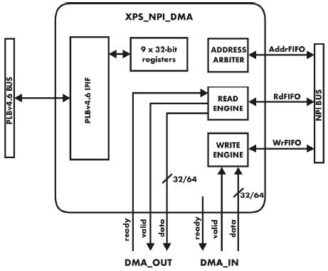
XPS_NPI_DMA is high performance direct memory access (DMA) engine which seamlessly integrates into Xilinx EDK environment (figure below). It is highly flexible due to full access of the softcore MicroBlaze to the XPS_NPI_DMA core functionality through 9 32-bit registers attached to PLBv4.6 bus.
...
| Scroll Title | ||
|---|---|---|
| ||
|
XPS_NPI_DMA Core Design Parameters
| Scroll Title | ||||||||||||||||||||||||||||||||||||||||||||||||||||||||||||||||||||||||||||||||||||||||||
|---|---|---|---|---|---|---|---|---|---|---|---|---|---|---|---|---|---|---|---|---|---|---|---|---|---|---|---|---|---|---|---|---|---|---|---|---|---|---|---|---|---|---|---|---|---|---|---|---|---|---|---|---|---|---|---|---|---|---|---|---|---|---|---|---|---|---|---|---|---|---|---|---|---|---|---|---|---|---|---|---|---|---|---|---|---|---|---|---|---|---|
| ||||||||||||||||||||||||||||||||||||||||||||||||||||||||||||||||||||||||||||||||||||||||||
| ||||||||||||||||||||||||||||||||||||||||||||||||||||||||||||||||||||||||||||||||||||||||||
XPS_NPI_DMA I/O Signal Descriptions
| Scroll Title | ||||||||||||||||||||||||||||||||||||||||||||||||||||||||||||||||||||||||||||||||||||||||||||||||||||||||||||||||||||||||||||||||||||||||||||||||||||||
|---|---|---|---|---|---|---|---|---|---|---|---|---|---|---|---|---|---|---|---|---|---|---|---|---|---|---|---|---|---|---|---|---|---|---|---|---|---|---|---|---|---|---|---|---|---|---|---|---|---|---|---|---|---|---|---|---|---|---|---|---|---|---|---|---|---|---|---|---|---|---|---|---|---|---|---|---|---|---|---|---|---|---|---|---|---|---|---|---|---|---|---|---|---|---|---|---|---|---|---|---|---|---|---|---|---|---|---|---|---|---|---|---|---|---|---|---|---|---|---|---|---|---|---|---|---|---|---|---|---|---|---|---|---|---|---|---|---|---|---|---|---|---|---|---|---|---|---|---|---|---|
| ||||||||||||||||||||||||||||||||||||||||||||||||||||||||||||||||||||||||||||||||||||||||||||||||||||||||||||||||||||||||||||||||||||||||||||||||||||||
|
Writing and reading to/from DMA_IN and DMA_OUT ports
The point to point unidirectional buses use simple handshaking protocol.
...
| Scroll Title | ||
|---|---|---|
| ||
|

XPS_NPI_DMA Core Registers
XPS_NPI_DMA has a full access of a microprocessor to the core functionality through a 9 user 32-bit and 7 IPIF Interrupt registers attached to PLBv4.6 bus.
...
| Note |
|---|
| The First (LSB) interrupt from user_logic is masked on the left!! |
Details of XPS_NPI_DMA Core Regi sters
The parts of the registers (or the whole registers) with a non-capital designation (e.g. wr_fifo_rst) are usually the names of the HDL signals connected to the described register.
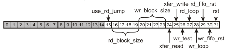
Control Register (CR)
The Control Register is used to control basic peripheral functions. All the bit flags are assembled here.
| Scroll Title | ||||||||||||||||||||||||||||||||||||||||||||||||
|---|---|---|---|---|---|---|---|---|---|---|---|---|---|---|---|---|---|---|---|---|---|---|---|---|---|---|---|---|---|---|---|---|---|---|---|---|---|---|---|---|---|---|---|---|---|---|---|---|
| ||||||||||||||||||||||||||||||||||||||||||||||||
|
Write Start Address Register (WSA)
Here, the user inputs start address for writing transfer. It is an external memory address for the first byte to be written.
...
| Scroll Title | ||
|---|---|---|
| ||
|

Write Bytes Register (WBR)
Here, the user inputs the number of bytes to written to memory. It is not necessary to align the number of bytes to block size, since the remaining bytes will be padded. If the user sets wr_loop to 1 then the WSA+WBR is the maximal address before the address counter jumps to WSA and starts counting again.
| Scroll Title | ||
|---|---|---|
| ||
|
Read Start Address Register (RSA)
Here, the user inputs start address for reading transfer. It is an external memory address for the first byte to be read.
...
| Scroll Title | ||
|---|---|---|
| ||
|
Read Bytes Register (RBR)
Here, the user inputs the number of bytes to be read from the memory. It is not necessary to align the number of bytes to block size, since the remaining bytes will remain in the RdFIFO. If the user sets rd_loop to 1 then the when the byte counter reaches RBR values jumps to 0 (RSA address) and starts counting again.
| Scroll Title | ||
|---|---|---|
| ||
|
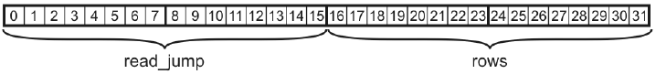
Read Jumps Register (RJR)
This register is used to input two16bit values to define the reading jumping startegy/algorithm. The read_jump is an address increment between two consecutive reads. If the user want linear read then this is a number of bytes per read block (4 or 8 for single beat xfer). When rotating (transposing) an image this should equal to number of bytes in a row. The parameter rows define how many reads should be done before returning to starting position+block size.
...
| Scroll Title | ||
|---|---|---|
| ||
|
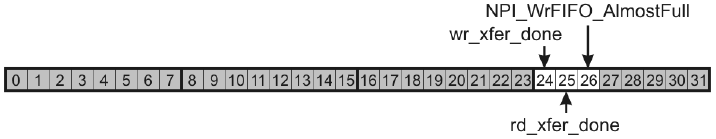
Status Register (SR)
In the status register the peripheral reports of the current status.
| Scroll Title | ||||||||||||||||
|---|---|---|---|---|---|---|---|---|---|---|---|---|---|---|---|---|
| ||||||||||||||||
|
Write Address Counter Register (WCR)
Reading this register returns current WRITE address counter value. It can be used to monitor write transfer progress.
| Scroll Title | ||
|---|---|---|
| ||
|
Read Address Counter Register (RCR)
Reading this register returns current READ address counter value. It can be used to monitor read transfer progress.
| Scroll Title | ||
|---|---|---|
| ||
|
Interrupt registers
With INTR_IPIER register the user can enable/disable peripheral interrupt sources. With INTR_IPISR the user can identify interrupt source. Writing a value to INTR_IPISR also clears interrupt.
...
| Scroll Title | ||
|---|---|---|
| ||
|
Programmin model
| Info |
|---|
| In the instruction sequence it is only important that xfer_write or xfer_read are written at the end as they start the transmission. |
...
| Scroll Title | ||||||||||||||||||||||||||||||||||||||||
|---|---|---|---|---|---|---|---|---|---|---|---|---|---|---|---|---|---|---|---|---|---|---|---|---|---|---|---|---|---|---|---|---|---|---|---|---|---|---|---|---|
| ||||||||||||||||||||||||||||||||||||||||
|
Example 1
Example of single write transfer from address 0x1C000000 to 0x1C00FFFF using 32-word burst
...
4. Poll SR until write_xfer_done = 1
Example 2
Example of single linear read transfer from address 0x1C000000 to 0x1C00FFFF using 32-word burst transaction
...
4. Poll SR until read_xfer_done = 1
Example 3
Example of single transpose read transfer from address 0x1C000000 at image size 750 bytes/row x 480 rows.
...
#projec t#(or IP repository)\drivers\xps_npi_dma_v1_00_a\src\xps_npi_dma.c
Example 4 (if Reference Design is used): test XPS_NPI_DMA and XPS_FX2 using MB Commands
XPS_NPI_DMA and XPS_FX2 custom IP blocks are both necessary to connect (throgh USB connection) host computer's software and TE USB FX2 module's DRAM.
...
Overview
Content Tools