Page History
| Scroll Ignore |
|---|
Download PDF Version of this Document. |
| Scroll pdf ignore | ||||
|---|---|---|---|---|
Table of Contents
|
...
| Scroll Only (inline) |
|---|
Online version of this manual and other related documents can be found at https://wiki.trenz-electronic.de/display/PD/TE0600
|
Trenz Electronic GigaBee XC6SLX series are industrial-grade FPGA micromodules integrating a leading-edge Xilinx Spartan-6 LX FPGA, Gigabit Ethernet transceiver (physical layer), two independent banks of 16-bit-wide 128/512 MBytes DDR3 SDRAM, 16 MBytes SPI Flash memory for configuration and operation, and powerful switch-mode power supplies for all on-board voltages. A large number of configurable I/Os is provided via robust board-to-board (B2B) connectors.
...
Storage device name | Content | Notes |
|---|---|---|
SPI Flash memory | Blinky Demo | |
protected 1-Wire EEPROM | not programmed |
Power Consumption
Power consumption of GigaBee XC6SLX modules highly depend on the FPGA design implemented. Some typical power consumptions are provided below for the following reference systems:
...
Unused IOB Pins option selection.
In the standard assembly, the /WDO (watchdog output) line is left unconnected1 and the only possibility to reset the module is by driving the /MR (master reset) line active (low) through pin 18 of connector J2.
...
| FPGA Bank | Single-ended | Differential | Total | VCCIO |
| Bank 0 | 1 | 22 | 45 | VCCIO 0 (3.3 V) |
| Bank 1 | 1 | 6 | 13 | VCCIO 1 (1.5 V) |
| Bank 2 | 3 | 21 | 45 | 3.3 V |
| Bank 3 | 0 | 3 | 6 | 1.5 V |
| 5 | 52 | 109 |
B2B signals count
Pin Labeling
...
Most pins of B2B connectors J1 and J2 are general-purpose, user-defined I/O pins (GPIOs). There are, however, up to 8 different functional types of pins on the TE0600, as outlined in Table below. In pin-out tables Table 11 and Table 12, the individual pins are colour-coded according to pin type as in Table below.
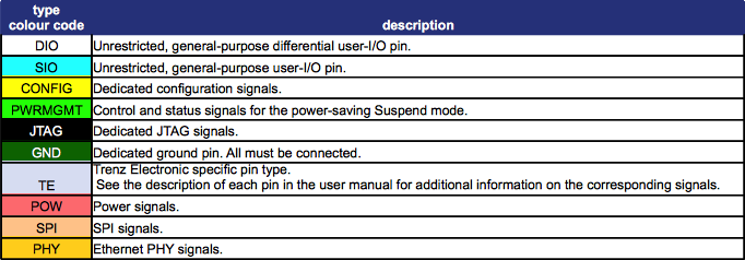
TE0600 pin types
| type colour code | description |
|---|---|
| DIO | Unrestricted, general-purpose differential user-I/O pin. |
| SIO | Unrestricted, general-purpose user-I/O pin. |
| CONFIG | Dedicated configuration signals. |
| PWRMGMT | Control and status signals for the power-saving Suspend mode. |
| JTAG | Dedicated JTAG signals. |
| GND | Dedicated ground pin. All must be connected. |
| TE | Trenz Electronic specific pin type. See the description of each pin in the user manual for additional information on the corresponding signals. |
| POW | Power signals. |
| SPI | SPI signals. |
| PHY | Ethernet PHY signals. |
...
Board revisions pin coding
Main differences between 01 and 02 revisions:
...
- Optimized placement and routing for DC/DC converters
- Added thermal vias to mounting holes
- Added Testpoints
- Changed Board revision identification to REV03
- Changed U9 from SIT1602AI-83-33E-25.0000 to SiT8008AI-73-XXS-25.000000E
- Added Track-it™ Traceability Pad
- Change SPI Flash from W25Q128BVEIG to W25Q128FVEIG
- DDR3 changed from IM4G16D3EABG-125I to IM4G16D3FABG-125I for the 4 GBit variants
- U13 (DS2432P+) is no longer populated by default
...
Module assembly variants coded by 4 zero ohm resistors, connected to FPGA AV[3:0] pins. All these pins should be configured to have internal PULLUP.
...
Xilinx DS160: Spartan-6 Family Overview
This overview outlines the features and product selection of the Spartan®-6 family.
http://www.xilinx.com/support/documentation/data_sheets/ds160.pdfXilinx DS162: Spartan-6 FPGA Data Sheet: DC and Switching Characteristics
This data sheet contains the DC and switching characteristic specifications for the Spartan®-6 family.
http://www.xilinx.com/support/documentation/data_sheets/ds162.pdfSamtec Razor Beam LSHM series overview.
http://www.samtec.com/LSHMMaxim DS2502-E48 product overview.
http://www.maxim-ic.com/datasheet/index.mvp/id/3748Winbond W25Q128BV product overview.
http://www.winbond.com/hq/enu/ProductAndSales/ProductLines/FlashMemory/SerialFlash/W25Q128BV.htmMaxim DS2432 product page.
http://www.maximintegrated.com/datasheet/index.mvp/id/2914
Documentation Archives
Xilinx Spartan-6 Documentation
http://www.xilinx.com/support/documentation/spartan-6.htmXilinx Documentation
http://www.xilinx.com/documentation/
http://www.xilinx.com/support/documentation/Trenz Electronic GigaBee Series Documentation
http://docs.trenz-electronic.de/Trenz_Electronic/products/TE0600-GigaBee_series/
...
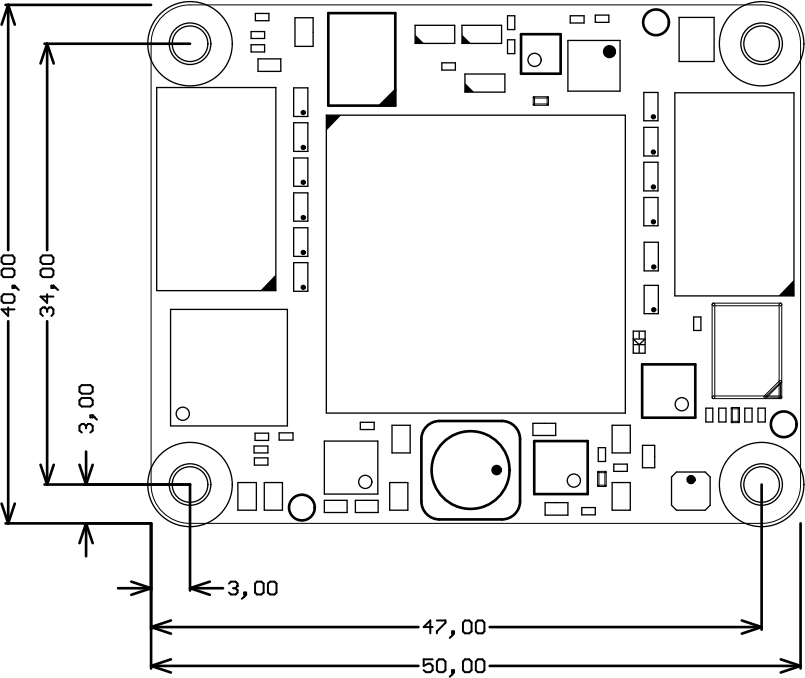
GigaBee XC6SLX has 4 mounting holes, one in each corner. The module can be fixed by screwing M3 screws (ISO 262) onto a carrier board through those mounting holes.
Operating Temperature Ranges
...
Date | Revision | Contributors | Description |
|---|---|---|---|
| 2011-10-01 | 0.01 | AIK | Release. |
| 2011-10-05 | 0.02 | AIK | Added B2B pin-out section. |
| 2011-10-06 | 0.03 | AIK | Reformatted pin-out tables. Added eFUSE programming section. |
| 2011-10-06 | 0.04 | AIK | Added board photos. Additions to eFUSE section. |
| 2011-10-06 | 0.05 | AIK | Removed net length information for nets which can't be measured right. |
| 2011-10-06 | 0.06 | AIK | Added power consumption section. |
| 2011-10-08 | 0.07 | AIK | Little fixes after FDR audit. |
| 2011-10-12 | 0.08 | AIK | Fix in eFUSE section. |
| 2011-11-11 | 0.09 | AIK | Added pin numbering description for B2B connectors |
| 2012-01-20 | 0.10 | AIK | Added pin compatibility note and manual reference. |
| 2012-04-12 | 0.11 | AIK | Added FPGA banks VCCIO voltages table. |
| 2012-04-17 | 1.00 | FDR | Updated documentation link. Replaced obsolete ElDesI and RedMine links with current GitHub links. Updated dating convention. |
| 2012-05-18 | 1.01 | AIK | Corrected cross-reference in section 3.2. Corrected LED description. |
| 2012-06-18 | 1.02 | FDR | Removed junction temperature limits under connector current ratings. |
| 2012-07-18 | 1.03 | AIK | Added table with B2B signals summary per FPGA bank |
| 2012-10-30 | 2.01 | AIK | Fork to 01 and 02 board revisions |
| 2012-11-06 | 2.01 | AIK | Fixed bank 1 power options |
| 2012-11-21 | 2.02 | AIK | Updated module diagram |
| 2012-11-30 | 2.03 | AIK | Added Ethernet disable note |
| 2012-12-19 | 2.04 | AIK | Fixed SPI Flash size on block diagram |
| 2013-01-21 | 2.05 | AIK | Added PHY reset note |
| 2013-03-13 | 2.06 | AIK | Connectors current chapter moved to separate document |
| 2013-03-13 | 2.07 | AIK | Changed Bank 1 power supply description and VCCIO0 sources description |
| 2016-01-29 | 2.08 | AIK | Pause advertise correction |
| 2016-11-05 | 3.00
| FDR | Document ported to wiki and adapted to web presentation. |
| 2017-04-03 | TT | Added REV03 to assembly Variant Table |
...
Overview
Content Tools