Page History
| Scroll Ignore |
|---|
Download PDF Version of this Document. |
| Scroll pdf ignore | |
|---|---|
Table of Contents
|
Overview
| Scroll Only (inline) |
|---|
Refer to https://shop.trenz-electronic.de/de/Download/?path=Trenz_Electronic/TE0725 for online version of this manual and other documents available about the product. |
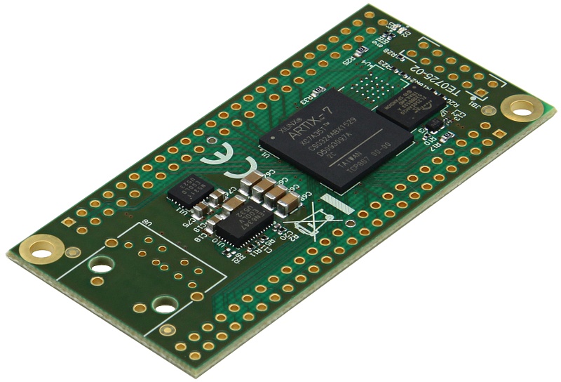
The Trenz Electronic TE0725 is a low cost small-sized FPGA module integrating a Xilinx Artix-7 (15-100T) and 32 MByte Flash memory for configuration and operation.
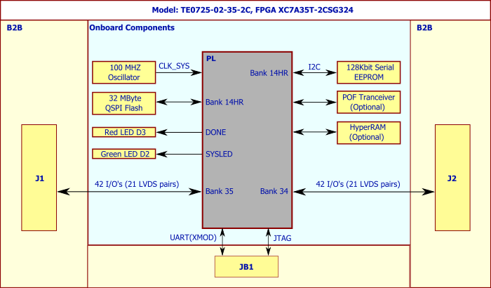
Block Diagram
| Page break |
|---|
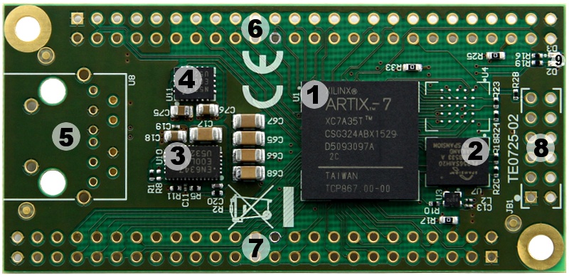
Main Components
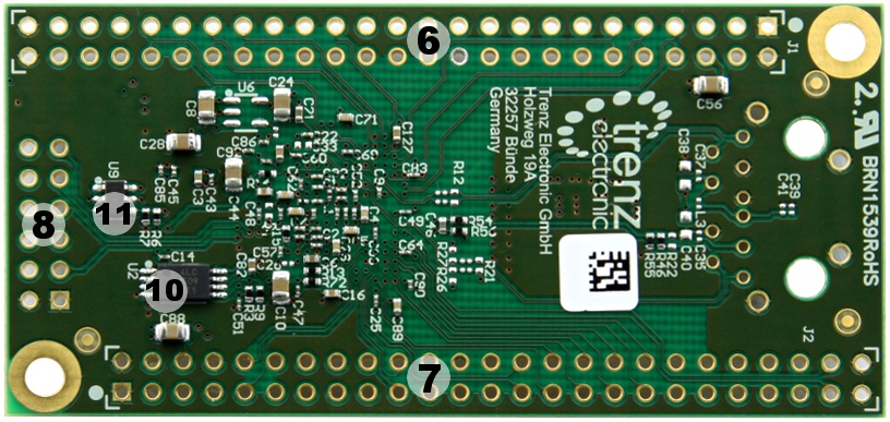
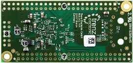
Note that on the images below, there is no POF transceiver, HyperRAM, 50-pin headers and JTAG/UART header installed on the module.
The 2 x 50 pin headers with a 2,54mm standard pitch are perfect for breadboard or low cost dual PCB design.
...
|
| |
| Top View | Bottom View |
- Xilinx Artix-7 FPGA, U1
- 32 MByte Flash Memory, U7
- Enpirion EN6347 4A PowerSoC DC-DC Step Down Converter, U10
- Enpirion EN5311 1A PowerSoC Synchronous Buck Regulator With Integrated Inductor, U11
- POF Tranceiver Placeholder, U8
- 50-pin placeholder for breadboard connection, J1
- 50-pin placeholder for breadboard connection, J2
- JTAG/UART connector, JB1
- Green LED D2(SYSLED) and Red LED D3(DONE)
- 16K x 8 (128 Kbit) Serial EEPROM, U2
- Ultralow Supply-Current Voltage Monitor With Optional Watchdog, U9
...
Xilinx Artix-7 XC7A35T (A15 to A100T)
Commercial Temperature Grade (Industrial on Request)
32 MByte Flash Memory
2 x 50 Pin Headers with 2,54mm Pitch, Ideal for Breadboard Use
- 87 IO's (42 + 42 + 3)
- 100 MHz System Clock
- I2C EEPROM
3.3V Single Power Supply with On-Board Voltage Regulators
Size 73 x 35 mm
JTAG/UART Connector
2 LED's
- Optional HyperRAM (8 to 32 MByte)
- Optional POF Fiber Optical Adapter (125, 250 or 1000MBit/s)
Initial Delivery State
...
Signals, Interfaces and Pins
...
I/O Banks
| Bank | VCCIO | B2B I/O | Notes |
|---|---|---|---|
| 0 | 3.3V | 0 | JTAG |
| 14 | 3.3V | 0 (3) | 3 I/O in XMOD-JTAG - for use as UART |
| 15 | 1.8V | 0 | used for optional hyper RAM |
| 16 | 2.5V | 0 | used for optional optical fiber tranceiver |
| 34 | User select | 42 | 0R resistor option to select 3.3V |
| 35 | User select | 42 | 0R resistor option to select 3.3V |
POF Transceiver

| Model | Bitrate MB/s | Notes |
|---|---|---|
AFBR-59F2Z | 250 |
JTAG Interface
JTAG access to the Xilinx Artix-7 device is provided through connector JB1.
| Signal | Pin Number |
|---|---|
| TCK | JB1: 4 |
| TDO | JB1: 8 |
| TDI | JB1: 10 |
| TMS | JB1: 12 |
Connector JB1 (2 x 6 pin Header) is directly compatible to XMOD JTAG Adapter TE0790. This adapter can be inserted from top onto the TE0725, if JB1 is fitted with male pin header. Optionally JB1 can be fitted with pin header from bottom, in that case the JTAG cable connector must be on the base board.
...
When using XMOD-JTAG please check the switch settings on XMOD to be sure the power and I/O reference are supplied correctly. TE0790 can in some case be used to power up TE0725, this is however not recommended. TE0790-01 has not enough power for TE0725 (LED Blink may work, for larger designs the XMOD delivered power may be not sufficient).
LED's
| LED | Color | FPGA | Notes |
|---|---|---|---|
| D2 | green | M16 | |
| D3 | red | DONE | Active Low |
...
All connectors are are for 100mil headers, all connector locations are in 100 mil grid.
| LED | Color | FPGA | |
|---|---|---|---|
| D2 | green | M16 | |
| D3 | red | DONE | Active Low |
Power and Power-On Sequence
For startup, a power supply with minimum current capability of 1A is recommended.
There is no specific or special power-on sequence, single power source is needed as VIN, rest of the sequence is automatic.
Power Supply
Single 3.3V Power supply required.
...
| FPGA | Design | Typical Power, 25C ambient |
|---|---|---|
| A35T | not configured | TBD |
| A35T | LED Blinky | 170mW (typical) |
| A100T | not configured | TBD |
TBD - To Be Determined.
Technical
...
Specifications
Absolute Maximum Ratings
Parameter | Min | Max | Units | Notes | Reference document |
|---|---|---|---|---|---|
Vin supply voltage | -0.1 | 3.6 | V | ||
| I/O Bank supply voltage | -0.5 | 3.6 | V | Xilinx document DS181 | |
| I/O input voltage for FPGA I/O banks | -0.4 | VCCO_X+0.55 | V | Xilinx document DS181 | |
| GT Transceiver | -0.5 | 1.26 | V | Xilinx document DS181 | |
Voltage on Module JTAG pins | -0.4 | VCCO_0+0.55 | V | VCCO_0 is 1.8V or 3.3V nominal | Xilinx document DS181 |
Storage Temperature | -40 | +85 | C |
Recommended Operating Conditions
| Parameter | Min | Max | Units | Notes | Reference document |
|---|---|---|---|---|---|
| Vin supply voltage | 3.135 | 3.45 | V | ||
| IO Bank supply voltage for I/O banks | 1.14 | 3.465 | V | Xilinx document DS181 | |
| I/O input voltage for I/O banks | -0.20 | VCCO + 0.20 | V | Xilinx document DS181 | |
| Voltage on Module JTAG pins | 3.135 | 3.465 | V | For assembly variant with 3.3V CONFIG Bank Option | Xilinx document DS181 |
| Note |
|---|
| Please check Xilinx datasheet for complete list of absolute maximum and recommended operating ratings for the Artix-7 device (DS181). |
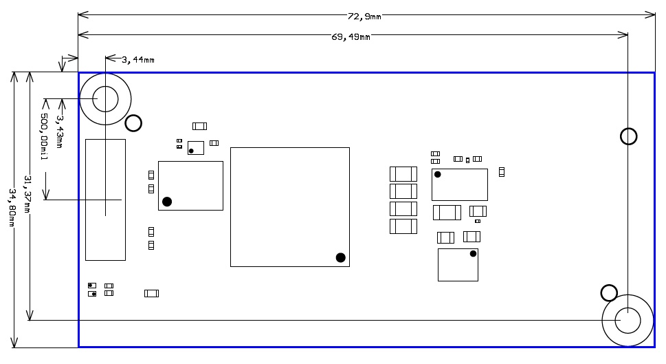
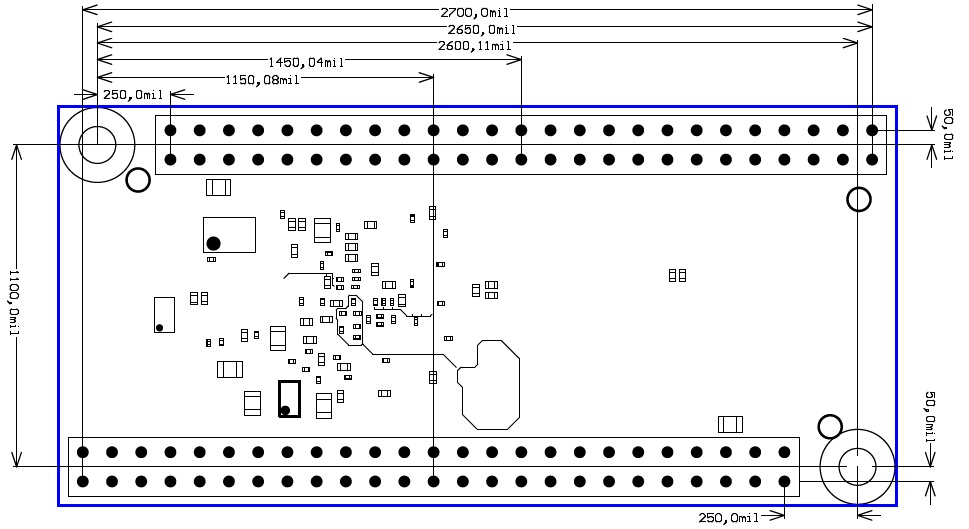
Physical Dimensions
Please note that two different units are used on the figures below, SI system millimeters(mm) and imperial system thousandth of an inch(mil). This is because of the 100mil pin headers used, see also explanation below. To convert mil's to millimeters and vise versa use formula 100mil's = 2,54mm.
|
| Top View |
|
Bottom View |
...
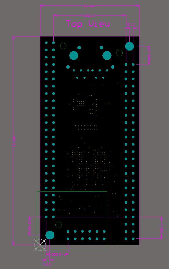
Measurements and placement of the connectors and mounting holes. All 100 mil pin headers are in 100 mil grid, the M3 mounting holes are in 50 mil grid aligned to the centers of the 100mil headers. The module is symmetrical, turning it 180 degrees will keep all I/O and Power Pins pins in both 50 pin headers in compatible places.
Operating Temperature Ranges
Commercial grade modules
All parts are at least commercial temperature range of 0°C to +70°C. The module operating temperature range depends on customer design and cooling solution. Please contact us for options.
Industrial grade modules
All parts are at least industrial temperature range of -40°C to +85°C. The module operating temperature range depends on customer design and cooling solution. Please contact us for options.
Weight
| Variant | Weight g | Note |
|---|---|---|
| 8.5 | Plain Module |
Revision History
Hardware Revision History
| Date | Revision | Notes | PCN | Documentation link |
|---|---|---|---|---|
| - | 01 | Prototypes | ||
| - | 02 | First production release |
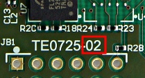
Hardware revision number is printed on the PCB board together with the module model number separated by the dash.
Document Change History
| Date | Revision | Contributors | Description |
|---|---|---|---|
| 2016-12-09 | Hardware Rev02 Block Diagram added | ||
| 2016-12-02 |
V1
| Initial version |
Disclaimer
| Include Page | ||||
|---|---|---|---|---|
|
Overview
Content Tools