Page History
...
| Page break |
|---|
Main Components
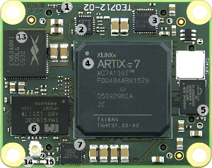
Programmable oscillator @25 MHz, SiTime SiT8008, U9
Programmable quad clock generator, Silicon Labs Si5338, U2
10/100 Mbps Ethernet PHY transceiver, Texas Instruments TLK106, U5
Xilinx Artix-7 FPGA XC7A series, U1
32 MByte QSPI Flash memory, Cypress S25FL256S, U4
4 Gbit DDR3 SDRAM, Intelligent Memory IM4G16D3EABG, U15
System Controller CPLD, Lattice Semiconductor MachXO2-256HC, U3
4 Gbit DDR3 SDRAM, Intelligent Memory IM4G16D3EABG, U19
Serial EEPROM, Microchip 11AA02E48, U7
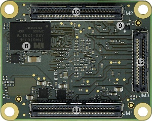
- Samtec Razor Beam™ LSHM-150 B2B connector, JM2
- Samtec Razor Beam™ LSHM-150 B2B connector, JM1
- Samtec Razor Beam™ LSHM-150 B2B connector, JM3
- 12A Enpirion EN63A0QI PowerSoC DC-DC converter, U14
- Green LED (SYSLED1), D1
- Red LED (SYSLED2), D2
Initial Delivery State
Programmable unit | Content | Notes |
|---|---|---|
| Xilinx Artix-7 FPGA | Not programmed | U1 |
| System Controller CPLD | Programmed | U3 |
| SPI Flash OTP area | Empty | U4 |
SPI Flash main array | Empty | U4 |
| SPI Flash Quad Enable bit | Set | U4 |
Microchip 11AA02E48 | Globally unique EUI-48 (Ethernet MAC address) | U7 |
Signals, Interfaces and Pins
...
FPGA bank number and number of I/O signals connected to the B2B connector:
| FPGA Bank | B2B Connector | I/O Signal Count | Voltage Level | Notes |
|---|---|---|---|---|
| 13 | JM1 | 10 | VCCIO13 | Supplied by the baseboard. Not available on XC7A35T assembly variant. |
| 13 | JM3 | 20 | VCCIO13 | Supplied by the baseboard. Not available on XC7A35T assembly variant. |
| 14 | JM1 | 8 | 3.3V | |
| 14 | JM2 | 18 | 3.3V | |
| 14 | JM3 | 4 | 3.3V | |
| 15 | JM2 | 48 | VCCIO15 | Supplied by the baseboard. |
| 15 | JM2 | 2 | VCCIO15 | Supplied by the baseboard. |
| 16 | JM1 | 48 | VCCIO16 | Supplied by the baseboard. |
Please refer to the Pin-out tables page for additional information.
...
JTAG access to the Xilinx Artix-7 FPGA and System Controller CPLD devices is provided through B2B connector JM2.
JTAG Signal | B2B Pin |
|---|---|
| TMS | JM2-93 |
| TDI | JM2-95 |
| TDO | JM2-97 |
| TCK | JM2-99 |
JTAGEN pin in B2B connector JM1 is used to select JTAG access for FPGA or SC CPLD:
...
Special purpose pins are connected to System Controller CPLD and have following default configuration:
| Pin Name | Mode | Function | Default Configuration |
|---|---|---|---|
| PGOOD |
| INOUT | Power good | Active low when EN1 is low or module power is invalid |
| otherwhise high impedance | |||
| JTAGEN | Input | JTAG select | Low for normal operation, high for System Controller CPLD access. |
| EN1 | Input | Power Enable | When forced low, pulls POR_B low to emulate power on reset. |
| NOSEQ | - | No function | Not used. |
| MODE | - | No function | Not used. |
Pin usages depends on Purpose of this IOs depends in the CPLD Firmware, please check also CPLD Firmware description, see: TE0712 CPLD
On-board LEDs
...
It is important that all baseboard I/Os are 3-stated at power-on until System Controller sets PGOOD signal high (B2B connector JM1, pin 30), or 3.3V is present on B2B connector JM2 pins 10 and 12, meaning that all on-module voltages have become stable and module is properly powered up.
...
Power Rail Name | B2B Connector JM1 Pin | B2B Connector JM2 Pin | Direction | Notes | |||
|---|---|---|---|---|---|---|---|
VIN | 1, 3, 5 | 2, 4, 6, 8 | Input | SoM supply voltage (from the baseboard). | |||
| 3.3VIN | 13, 15 | - | Input | SoM supply voltage (from the baseboard). | |||
| 1.5V | - | 19 | Output | Module internal 1.5V level. | |||
1.8V | 39 | - | Output | Module internal 1.8V level. Maximum 300mA available. | |||
| 3.3V14 | - | 10, 12 | Output | Module internal 3.3V level. | |||
| 3.3V | VCCIO1314 | -Output | Module internal 3.3V level. Not on all 4x5 modules | ||||
| VCCIO13 | - | 1, 3 | Input | High-Range | 1, 3 | Input | High-Range bank supply voltage (from the baseboard). |
| VCCIO15 | - | 7, 9 | Input | High-Range bank supply voltage (from the baseboard). | |||
| VCCIO16 | 9, 11 | - | Input | High-Range bank supply voltage (from the baseboard). | |||
| VREF_JTAG | - | 91 | Output | JTAG reference voltage (3.3V). |
...
Date | Revision | Contributors | Description | ||||||||||||||||||||||||||
|---|---|---|---|---|---|---|---|---|---|---|---|---|---|---|---|---|---|---|---|---|---|---|---|---|---|---|---|---|---|
|
|
|
| ||||||||||||||||||||||||||
| 2017-12-15 | v.18 | John Hartfiel |
| ||||||||||||||||||||||||||
| 2017-12-12 | v15v.15 | John Hartfiel |
| ||||||||||||||||||||||||||
| 2017-05-29 | v.13 | Jan Kumann |
| ||||||||||||||||||||||||||
| 2017-03-01 | v.7 | John Hartfiel |
| ||||||||||||||||||||||||||
| 2017-01-26 | v.3 | Jan Kumann |
| ||||||||||||||||||||||||||
| 2017-01-20 | v.2
| Jan Kumann |
| ||||||||||||||||||||||||||
| 2013-12-02 | v.1 | Antti Lukats |
| ||||||||||||||||||||||||||
| -- | all |
|
|
Disclaimer
| Include Page | ||||
|---|---|---|---|---|
|
Overview
Content Tools