Page History
...
The Si5338 can be programmed to change the output frequency of the FPGA clocks (the Ethernet clock must remain at 50 MHz). An I2C bus is connected between the FPGA (master) and clock generator (slave). Proper logic needs to be created in the FPGA to exercise the I2C bus with the correct data. See the reference design section for more information.
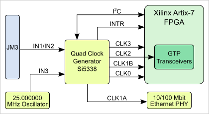
| CLK Output | FPGA Bank | FPGA Pin | IO Standard | Net Name | Default Frequency REV 01, REV 02 | Default Frequency REV 03 and higher | Notes |
|---|---|---|---|---|---|---|---|
| CLK0 | 35 | K4/J4 | DIFF_SSTL15 | CLK0_P/N | Off | 100MHz LVDS18 | NB! Since PCB REV02. |
| CLK1A | - | - | CLK50M | 50 MHz | 50MHz CMOS33 | PHY chip RMII reference clock. | |
| CLK1B | 34 | R4 | CLK50M2 | Off | 50MHz CMOS33 | NB! Since PCB REV02. | |
| CLK2 | 216 | F6/E6 | Auto | MGT_CLK0_P/N | 125 MHz | 125MHz LVDS18 | GTP transceiver clock. |
| CLK3 | 35 | H4/G4 | DIFF_SSTL15 | PLL_CLK_P/N | 50 MHz | 50MHz LVDS18 |
Certain B2B connector pins are connected to the FPGA pins which are capable of handling clocking signals from the user’s PCB (baseboard). See schematics B2B page for additional information.
...
Overview
Content Tools