Page History
| Scroll Ignore |
|---|
Download PDF Version version of this Documentdocument. |
| Scroll pdf ignore | |
|---|---|
Table of Contents
|
...
| Scroll Only (inline) |
|---|
Refer to https://shop.trenz-electronic.de/de/Download/?path=Trenz_Electronic/TE0725 for onlinedownloadable version of this manual and otheradditional documentstechnical availabledocumentation aboutof the product. |
The Trenz Electronic TE0725 is a low cost small-sized FPGA module integrating a Xilinx Artix-7 (15-100T) and 32 MByte Flash memory for configuration and operation.
...
- Xilinx Artix-7 FPGA, U1
- 32 MByte Flash Memory, U7
- Enpirion EN6347 4A PowerSoC DC-DC Step Down Converter, U10
- Enpirion EN5311 1A PowerSoC Synchronous Buck Regulator With Integrated Inductor, U11
- POF Tranceiver Transceiver Placeholder, U8
- 50-pin placeholder for breadboard connection, J1
- 50-pin placeholder for breadboard connection, J2
- JTAG/UART connector, JB1
- Green LED D2(SYSLED) and Red LED D3(DONE)
- 16K x 8 (128 Kbit) Serial EEPROM, U2
- Ultralow Supply-Current Voltage Monitor With Optional Watchdog, U9
...
Xilinx Artix-7 XC7A35T (A15 to A100T)
Commercial Temperature Grade (Industrial on Request)
32 MByte Flash Memory
2 x 50 Pin Headers with 2,54mm Pitch, Ideal for Breadboard Use
- 87 IO's (42 + 42 + 3)
- 100 MHz System Clock
- I2C EEPROM
3.3V Single Power Supply with On-Board Voltage Regulators
Size 73 x 35 mm
JTAG/UART Connector
2 LED's
- Optional HyperRAM (8 to 32 MByte)
- Optional POF Fiber Optical Adapter (125, /250 or 1000MBitMBit/s)
Signals, Interfaces and Pins
I/O Banks
| Bank | VCCIO | B2B I/O | Notes |
|---|---|---|---|
| 0 | 3.3V | 0 | JTAG |
| 14 | 3.3V | 0 (3) | 3 I/O in XMOD-JTAG - for use as UART |
| 15 | 1.8V | 0 | used for optional hyper RAM |
| 16 | 2.5V | 0 | used for optional optical fiber tranceiver |
| 34 | User select | 42 | 0R resistor option to select 3.3V |
| 35 | User select | 42 | 0R resistor option to select 3.3V |
...
Power and Power-On Sequence
For startup, a To power-up a module, power supply with minimum current capability of 1A is recommended.
There is no specific or special power-on sequence, single power source is needed as VIN, rest of the sequence is automatic.
Power Supply
Power Supply
TE0725 needs one single power supply with nominal of 3.3VSingle 3.3V Power supply required.
Power Consumption
| FPGA | Design | Typical Power, 25C ambient |
|---|---|---|
| A35T | not configured | TBD |
| A35T | LED Blinky | 170mW (typical) |
| A100T | not configured | TBD |
TBD - To Be Determined.
Actual power consumption depends on the FPGA design and ambient temperature.
Power-On Sequence
There is no specific or special power-on sequence, single power source is needed as VIN, rest of the sequence is automatic.
Variants Currently In Production
| Module Variant | FPGA Chip Model | PL Clock [MHz] | VIN Supply Voltage [V] | SPI Flash | HyperRAM |
|---|---|---|---|---|---|
TE0725-03-35-2C | XC7A35T-2CSG324C | 100 | 3.3V | S25FL256S | 8 MByte |
TE0725-03-100-2C | XC7A100T-2CSG324C | 100 | 3.3V | S25FL256S | 8 MByte |
TE0725-03-100-2I9 | XC7A100T-2CSG324I | 100 | 3.3V | S25FL256S | 8 MByte |
Technical Specifications
Absolute Maximum Ratings
Parameter | Min | Max | Units | Notes | Reference document |
|---|---|---|---|---|---|
VIN supply voltage | -0.1 | 3.6 | V | ||
| I/O Bank supply voltage | -0.5 | 3.6 | V | Xilinx document DS181 | |
| I/O input voltage for FPGA I/O banks | -0.4 | VCCO_X+0.55 | V | Xilinx document DS181 | |
| GT Transceiver | -0.5 | 1.26 | V | Xilinx document DS181 | |
Voltage on Module JTAG pins | -0.4 | VCCO_0+0.55 | V | VCCO_0 is 1.8V or 3.3V nominal | Xilinx document DS181 |
Storage Temperature | -40 | +85 | C°C |
Recommended Operating Conditions
...
| Date | Revision | Notes | PCN | Documentation link | ||
|---|---|---|---|---|---|---|
| 2016-12-09 | 0103 | Prototypes | Second production release | Click to see PCN | TE0725 | |
| - | 02 | First production release | TRM-TE0725 | TRM-02 | 2016-12||
| - | 0903 | 01 | Second production release | Prototypes | Click to see PCN |
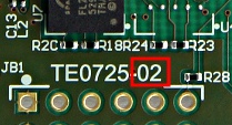
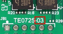
Hardware revision number is printed on the PCB board together with the module model number separated by the dash.
Document Change History
| Date | Revision | Contributors | Description |
|---|---|---|---|
| 2016-12-0915 | Hardware REV03 specific information added | ||
| 2016-12-09 | V40 | Hardware REV02 Block Diagram added | |
| 2016-12-02 | V1
| Initial version |
...
Overview
Content Tools