Page History
...
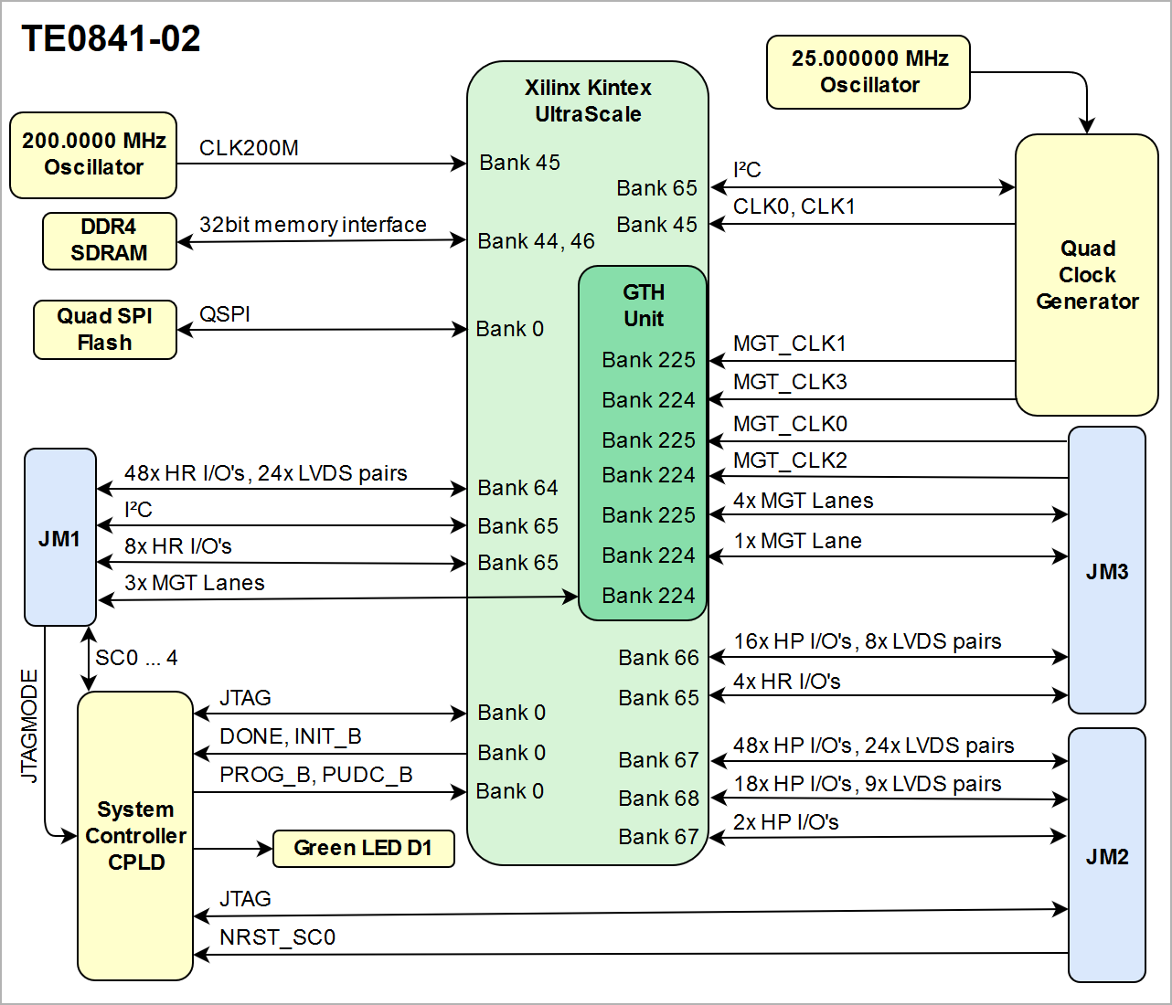
- Xilinx Kintex UltraScale FPGA (XCKU035 or XCKU040)
- 2 banks of 1024 MByte DDR4 SDRAM, 32bit wide memory interface(each DDR 16bit separate)
- 512 Mbit (64 MByte) QSPI Flash
- 3 x Samtec Razor Beam LSHM B2B, 260 terminals total
- 60 x HR I/Os
- 84 x HP I/Os
- 8 x GTH transceiver lanes (TX/RX)
- 2 x MGT external clock inputs - Clocking
- Si5338 - 4 output PLLs, GT and PL clocks
- 200 MHz LVDS oscillator - All power supplies on-board, single power source operation
- Evenly spread supply pins for optimized signal integrity
- Size: 40 x 50 mm
- 3 mm mounting holes for skyline heat spreader
- Rugged for industrial applications
...
| Scroll Title | ||||||||||||||||||||||||||||||||||
|---|---|---|---|---|---|---|---|---|---|---|---|---|---|---|---|---|---|---|---|---|---|---|---|---|---|---|---|---|---|---|---|---|---|---|
| ||||||||||||||||||||||||||||||||||
|
Main Components
| Scroll Title | ||||||||||||||||||||||||||||||||||||
|---|---|---|---|---|---|---|---|---|---|---|---|---|---|---|---|---|---|---|---|---|---|---|---|---|---|---|---|---|---|---|---|---|---|---|---|---|
| ||||||||||||||||||||||||||||||||||||
|

...
- Xilinx Kintex UltraScale FPGA, U1
- Ultra performance oscillator @25.000000 MHz, U3
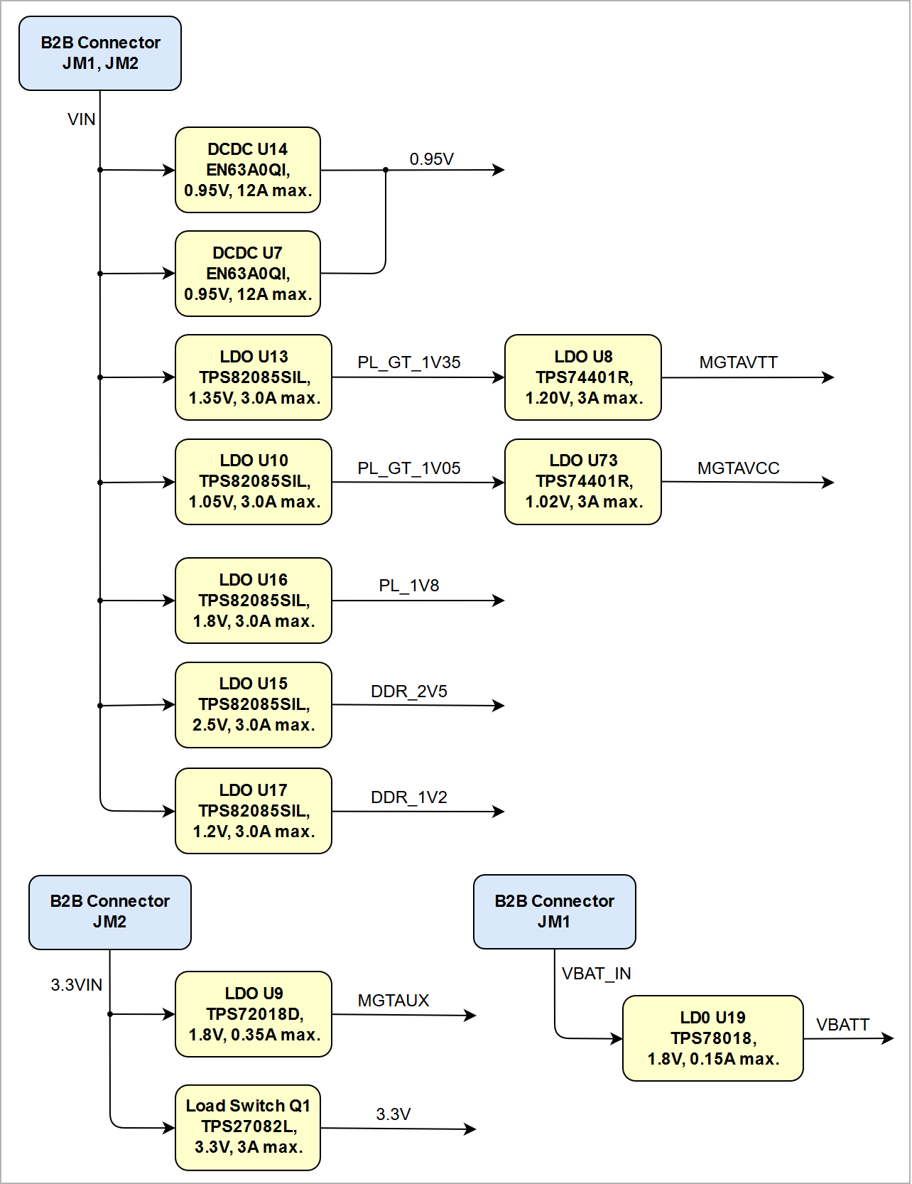
- 12A PowerSoC DC-DC converter (0.95V), U14
- 12A PowerSoC DC-DC converter (0.95V), U7
Low-jitter precision LVDS oscillator @200.0000 MHz, U11
- Low-dropout (LDO) linear regulator (MGTAVTT 1.20V), U8
- Low-dropout (LDO) linear regulator (MGTAVCC 1.02V), U12
- Samtec Razor Beam™ LSHM-150 B2B connector, JM1
- Samtec Razor Beam™ LSHM-150 B2B connector, JM2
- Samtec Razor Beam™ LSHM-130 B2B connector, JM3
- Programmable quad clock generator, U2
- 64 MByte QSPI Flash, U6
- 8 Gbit DDR4 SDRAM, U4
- 8 Gbit DDR4 SDRAM, U5
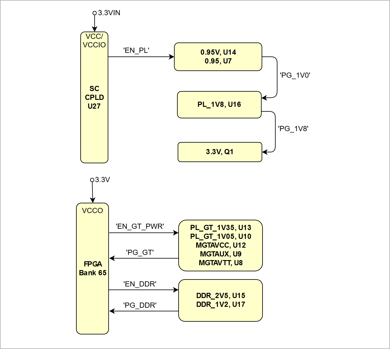
- System Controller CPLD, U18Programmable Clock Generator
- Low-dropout (LDO) linear regulator (MGTAUX), U9
- Ultra-low power low-dropout (LDO) regulator (VBATT), U19
...
Storage device name | Content | Notes | |
|---|---|---|---|
System Controller CPLD | Default firmware | - | |
| OTP Flash area | Empty | Not programmed | |
| Quad clock generator OTP area | Empty | programmed | on PCB REV02 and newerNot programmed |
Table 1: TE0841-02 module initial delivery state of programmable on-board devices
...
| Scroll Title | |||||||||||||||||||||||||||||||||||
|---|---|---|---|---|---|---|---|---|---|---|---|---|---|---|---|---|---|---|---|---|---|---|---|---|---|---|---|---|---|---|---|---|---|---|---|
| |||||||||||||||||||||||||||||||||||
|
See also Xilinx datasheet DS892 for additional information. User should also check related base board documentation when intending base board design for TE0841 module.
...
| Scroll Title | ||||||||||||||||||||||||||||||||||
|---|---|---|---|---|---|---|---|---|---|---|---|---|---|---|---|---|---|---|---|---|---|---|---|---|---|---|---|---|---|---|---|---|---|---|
| ||||||||||||||||||||||||||||||||||
|
Power Rails
| Power Rail Name | B2B JM1 Pins | B2B JM2 Pins | Input/Output | Notes |
|---|---|---|---|---|
| VIN | 1, 3, 5 | 2, 4, 6, 8 | Input | Supply voltage. |
| 3.3VIN | 13, 15 | - | Input | Supply voltage. |
| B64_VCO | 9, 11 | - | Input | HR (High Range) bank voltage. |
| B66_VCO | - | 1, 3 | Input | HP (High Performance) bank voltage. |
| B67_VCO | - | 7, 9 | Input | HP (High Performance) bank voltage. |
| B68_VCO | - | 5 | Input | HP (High Performance) bank voltage. |
VBAT_IN | 79 | - | Input | RTC battery supply voltage. |
| 3.3V | - | 10, 12, 91 | Output | Module on-board 3.3V voltage level. |
...
Table 14: Module PL I/O bank voltages
Board to Board Connector
| Include Page | ||||
|---|---|---|---|---|
|
Variants Currently In Production
| HTML |
|---|
<!-- GenerateSet new entry: Replace with correct on for selected module series --> |
...
Variants Currently In Production
| HTML |
|---|
<!-- Set correct link to the correct link to the overview table of the product on english and german, if not available, set https://shop.trenz-electronic.de/de/Produkte/Trenz-Electronic/ https://shop.trenz-electronic.de/en/Products/Trenz-Electronic/ --> |
...
Parameter | Min | Max | Units | Reference Document |
|---|---|---|---|---|
VIN supply voltage | -0.3 | 6.0 | V | EN63A0QI, TPS74401RGW datasheets |
| 3.3VIN supply voltage | -0.1 | 3.4 | V | Xilinx datasheet DS892 (HR Bank VCCO) |
| VBAT_IN | -0.3 | 6.0 | V | TPS780xx datasheet |
| Supply voltage for HR I/O banks (VCCO) | -0.500 | 3.400 | V | Xilinx datasheet DS892 |
Supply voltage for HP I/O banks (VCCO) | -0.500 | 2.000 | V | Xilinx datasheet DS892 |
| I/O input voltage for HR I/O banks | -0.400 | VCCO + 0.550 | V | Xilinx datasheet DS892 |
I/O input voltage for HP I/O banks | -0.550 | VCCO + 0.550 | V | Xilinx datasheet DS892 |
| I/O input voltage for SC CPLD U18 | -0.5 | 3.75 | V | LCMXO2-256HC datasheet |
| GTH and GTY transceiver reference clocks absolute input voltage (MGT_CLK0, MGT_CLK2) | -0.500 | 1.320 | V | Xilinx datasheet DS892 |
GTH and GTY transceiver receiver (RXP/RXN) and transmitter (TXP/TXN) absolute input voltage | -0.500 | 1.260 | V | Xilinx datasheet DS892 |
Storage temperature | -40 | +100 | °C | SML-P11 LED datasheet |
...
| Parameter | Min | Max | Units | Reference Document |
|---|---|---|---|---|
| VIN supply voltage | 3.3 | 5.5 | V | TPS82085SIL, TPS74401RGW datasheet |
| 3.3VIN supply voltage | 3.3 | 3.4 | V | Xilinx datasheet DS892 (HR Bank VCCO) |
| VBAT_IN | 2.2 | 5.5 | V | TPS780xx datasheet |
| Supply voltage for HR I/O banks (VCCO) | 1.140 | 3.400 | V | Xilinx datasheet DS892 |
Supply voltage for HP I/O banks (VCCO) | 0.950 | 1.890 | V | Xilinx datasheet DS892 |
I/O input voltage for HR I/O banks | –0.200 | VCCO + 0.20 | V | Xilinx datasheet DS892 |
| I/O input voltage for HP I/O banks | –0.200 | VCCO + 0.20 | V | Xilinx datasheet DS892 |
| I/O input voltage for SC CPLD U18 | -0.3 | 3.6 | V | LCMXO2-256HC datasheet |
Industrial Module Operating Temperature Range | -40 | 85 | °C | Xilinx datasheet DS892 |
| Commercial Module Operating Temperature Range | 0 | 85 | °C | Xilinx DS892, Silicon Labs Si5338 datasheet |
...
| HTML |
|---|
<!-- Generate new entry: 1.add new row below first 2.Copy "Page Information Macro(date)" Macro-Preview, Metadata Version number, Author Name and description to the empty row. Important Revision number must be the same as the Wiki document revision number 3.Update Metadata = "Page Information Macro (current-version)" Preview+1 and add Author and change description. --> |
...
Date | Revision | Contributors | Description | ||||||||||||||||||||||||||
|---|---|---|---|---|---|---|---|---|---|---|---|---|---|---|---|---|---|---|---|---|---|---|---|---|---|---|---|---|---|
|
|
|
| ||||||||||||||||||||||||||
| 2018-08-07 | v.69 | Ali Naseri |
| ||||||||||||||||||||||||||
| 2018-07-13 | v.68 | Ali Naseri |
| ||||||||||||||||||||||||||
2018-07-10 | v.58 | John Hartfiel |
| ||||||||||||||||||||||||||
2018-03-13 | v.57 | Jan Kumann, Ali Naseri |
| ||||||||||||||||||||||||||
| -- | all |
|
|
Table 18: Document change history.
Disclaimer
| Include Page | ||||
|---|---|---|---|---|
|
Overview
Content Tools