Page History
...
Additional assembly options are available for cost or performance optimization upon request.
Initial Delivery State
Programmable unit | Content | Notes |
|---|---|---|
| Xilinx Artix-7 FPGA | Not programmed | U1 |
| System Controller CPLD | Programmed | U3 |
| SPI Flash OTP area | Empty | U4 |
SPI Flash main array | Empty | U4 |
| SPI Flash Quad Enable bit | Set | U4 |
Signals, Interfaces and Pins
...
FPGA banks and I/O signals connected to the B2B connectors:
| FPGA Bank | B2B Connector | I/O Signal Count | Voltage Level | Notes |
|---|---|---|---|---|
| 13 | JM1 | 14 | VCCIO13 | Supplied by the baseboard. |
| 13 | JM2 | 18 | VCCIO13 | Supplied by the baseboard. |
| 13 | JM3 | 2 | VCCIO13 | Supplied by the baseboard. |
| 14 | JM1 | 8 | 3.3V | |
| 14 | JM3 | 12 | 3.3V | |
| 15 | JM2 | 48 | VCCIO15 | Supplied by the baseboard. |
| 15 | JM2 | 2 | VCCIO15 | Supplied by the baseboard. |
| 16 | JM1 | 48 | VCCIO16 | Supplied by the baseboard. |
JTAG Interface
JTAG access to the Xilinx Artix-7 FPGA and System Controller CPLD devices is provided through B2B connector JM2.
JTAG Signal | B2B Pin |
|---|---|
| TMS | JM2-93 |
| TDI | JM2-95 |
| TDO | JM2-97 |
| TCK | JM2-99 |
JTAGEN pin in B2B connector JM1 is used to select JTAG access for FPGA or SC CPLD:
| JTAGEN | JTAG Access To |
|---|---|
| Low | Artix-7 FPGA |
| High | System Controller CPLD |
System Controller I/O Pins
Special purpose pins are connected to System Controller CPLD and have following default configuration:
| Pin Name | Mode | Function | Default Configuration |
|---|---|---|---|
| PGOOD | Output | Power good | Active high when all on-module power supplies are working properly. |
| JTAGEN | Input | JTAG select | Low for normal operation, high for System Controller CPLD access. |
| EN1 | Input | Power Enable | When forced low, pulls POR_B low to emulate power on reset. |
| NOSEQ | - | No function | Not used. |
| MODE | - | No function | Not used. |
LEDs
The TE0713-01 module has one LED which is connected to the System Controller CPLD. Once FPGA configuration has completed, it can be used by the user's design.
| LED | Color | SC Signal | SC Pin | Notes |
|---|---|---|---|---|
| D1 | Green | SYSLED1 | 8 | Exact function is defined by SC CPLD firmware. |
Clocking
Si5338 programmable clock generator chip is used to generate clocks with 25 MHz oscillator as input connected to the pin IN3. There is a I2C bus connected between the FPGA bank 14 (master) and clock generator chip (slave) which can be used to program output frequencies. See the reference design for more information.
...
See Xilinx datasheet DS181 - "Artix-7 FPGAs Data Sheet: DC and AC Switching Characteristics" for additional information. User should also check related baseboard documentation when choosing baseboard design for TE0713 module.
Power Rails
Power Rail Name | B2B Connector JM1 Pin | B2B Connector JM2 Pin | Direction | Notes |
|---|---|---|---|---|
VIN | 1, 3, 5 | 2, 4, 6, 8 | Input | SoM supply voltage (from the baseboard). |
| 3.3VIN | 13, 15 | - | Input | SoM supply voltage (from the baseboard). |
| DDR_PWR | - | 19 | Output | Module internal 1. |
| 35V level. | ||||
1.8V | 39 | - | Output | Module internal 1.8V level. Maximum 300mA available. |
| 3.3V | - | 10, 12 | Output | Module internal 3.3V level. |
| VCCIO13 | - | 1, 3 | Input | High-Range bank supply voltage (from the baseboard). |
| VCCIO15 | - | 7, 9 | Input | High-Range bank supply voltage (from the baseboard). |
| VCCIO16 | 9, 11 | - | Input | High-Range bank supply voltage (from the baseboard). |
| VREF_JTAG | - | 91 | Output | JTAG reference voltage (3.3V). |
Board to Board Connectors
...
Technical Specifications
Absolute Maximum Ratings
Parameter | Min | Max | Units | Reference Document |
|---|---|---|---|---|
VIN supply voltage | V | |||
| 3.3VIN supply voltage | V | |||
Storage temperature (ambient) | -55 | 100 | °C | See IM4G16D3FABG datasheet. |
Recommended Operating Conditions
| Parameter | Min | Max | Units | Reference Document |
|---|---|---|---|---|
| VIN supply voltage | V | |||
| 3.3VIN supply voltage | V |
| Note |
|---|
| Assembly variants for higher storage temperature range are available on request. |
...
Hardware Revision History
| Date | Revision | Notes | PCN | Documentation Link |
|---|---|---|---|---|
| 2016-06-30 | 01 | First production revision | TE0713-01 |
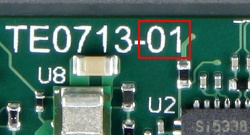
Hardware revision number is printed on the PCB board together with the module model number separated by the dash.
Document Change History
Date | Revision | Contributors | Description |
|---|---|---|---|
| 2017-02-07 | Jan Kumann | Initial document. |
Disclaimer
| Include Page | ||||
|---|---|---|---|---|
|
Overview
Content Tools