Page History
...
The JTAG-interface of the mounted 4 x 5 SoM can be accessed via header JX1. This header has a 'XMOD FTDI JTAG Adapter'-compatible pin-assignment.
| JX1 pin | JX1 pin net-name | B2B |
|---|---|---|
| C (pin 4) | TCK | JB3-100 |
| D (pin 8) | TDO | JB3-98 |
| F (pin 10) | TDI | JB3-96 |
| H (pin 12) | TMS | JB3-94 |
| A (pin 3) | MIO15 | JB1-86 |
| B (pin 7) | MIO14 | JB1-91 |
| E (pin 9) | BOOTMODE |
| JB1-90 (JTAGSELECT) | ||
| G (pin 11) | RESIN | JB3-17 |
Table 3: JTAG header JX1 pin-assignment
...
The external power-supply can be connected to the board by the following pins:
| Connector | 3.3V pin | GND pin |
|---|---|---|
| JX1 | JX1-5, JX1-6, | JX1-1, JX1-2 |
| J3 | J3-5, J3-6 | J3-1, J3-2 |
| J4 | J4-5 | J4-1, J4-2 |
| J20 | J20-5, J20-46 | J20-1 , J20-2 , J20-49 , J20-50 |
| J17 | J17-5, J17-46 | J17-1 , J17-2 , J17-49 , J17-50 |
Table 4: Connector-pins capable for external 3.3V power-supply
...
Summary of VCCIO-configuration
On the TE0705 TEBA0841 carrier board all the PL IO-bank's supply voltages of the 4x5 SoM (VCCIOA, VCCIOB, VCCIOC, VCCIOD; see 4x5 Module Integration Guide) are connected to the base-board VCCIO-voltage VIOTB, which is either fixed to 3.3V (J21: 1-2, 3) or selectable with the adjustable supply-voltage VADJ (J21: 1, 2-3). The supply-voltages have following pin-assignments on B2B-connectors:
VCCIOA and VCCIOA, which are selectable between the supply-voltages 1.8V, 2.5V and 3.3V via jumper J26 and J27
baseboard supply-voltages | base-board B2B connector-pins |
|---|
base-board
...
| base-board B2B connector- |
|---|
...
| pinsstandard assignment of PL IO-bank supply-voltages on TE 4x5 module's B2B connectors |
|---|
...
base-board voltages and signals connected with
| VCCIOA | JB1-10, JB1-12 |
...
...
| VCCIOA (JM1- |
...
| 9, |
...
| JM1-11) | |
| VCCIOD | JB2-8, JB2-10 |
VCCIOA (JM1-9, JM1-11),
VCCIOB (JM2-1, JM2-3), VCCIOC (JM2-5),
| VCCIOD (JM2-7, JM2-9) |
Table 4: base-board supply-voltages VCCIOA and VCCIOD
VCCIO3 (Systm-Controller-CPLD pin 5, 11, 23),
J15 VTREF,
J11, J13, J2, J5 and J6 VCCIO
Table 4: base-board supply-voltage VIOTB
| Note |
|---|
Note: The corresponding PL IO-voltage supply voltages of the 4x5 SoM to the selectable base-board voltage VIOTB are depending on the mounted 4x5 SoM and varying in order of the used model. Refer to SoM's schematic to get information about the specific pin-assignment on module's B2B-connectors regarding PL IO-bank supply voltages and to the 4x5 Module integration Guide for VCCIO voltage options. |
Following table describes how to configure the base-board supply-voltages by jumpers:
base-board supply-voltages vs voltage-levels |
|---|
| VCCIOA |
|---|
| VCCIOD | |
|---|---|
| 1.8V | J26:1-2 |
| J27 |
| :1 |
| -2 |
(J20: 1-2: additional decoupling-capacitor 100 µF)
| 2.5V | J26:3-4 | J27:3-4 |
| 3.3V | J26:5-6 | J27:5-6 |
Table 5: Configuration of base-board supply-voltages via jumpers. Jumper-Notification: 'Jx: 1-2, 3' means pins 1 and 2 are connected, 3 is open. 'Jx: 1, 23-34' means pins 2 3 and 3 4 are connected, 1 is openand so on.
| Note |
|---|
| It is recommended to set and measure the PL IO-bank supply-voltages before mounting of TE 4x5 module to avoid failures and damages to the functionality of the mounted SoM. |
Technical Specifications
Absolute Maximum Ratings
...
Board size: PCB 170.4 mm × 98 mm. Notice that some parts the are hanging slightly over the edge of the PCB like the mini USB-jacks (ca. 1.4 mm) and the Ethernet RJ-45 jack (ca 2.2 mm), which determine the total physical dimensions of the carrier board. Please download the assembly diagram for exact numbers.
Mating height of the module with standard connectors: 8mm
PCB thickness: ca. 1.65mm
Highest part on the PCB is the Ethernet RJ-45 jackSFP+ connector, which has an approximately 17 mm overall hight. Please download the step model for exact numbers.
All dimensions are given in mm.
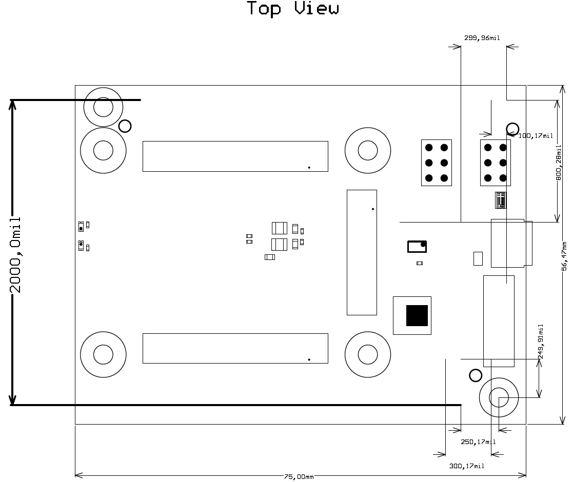
Figure 4: Physical Dimensions of the TE0705-04 carrier board
...
Overview
Content Tools