Page History
...
The Trenz Electronic TEBA0841 Carrier Board is a base-board for 4 x5 4 x 5 SoMs, which is dedicated to test- and evaluation-purposes of Multi-gigabit transceiver units of Trenz Electronic 4x5 SoMs.
...
See page "4 x 5 cm carriers" to get information about the SoMs supported by the TEBA0841 Carrier Board.
Block Diagram
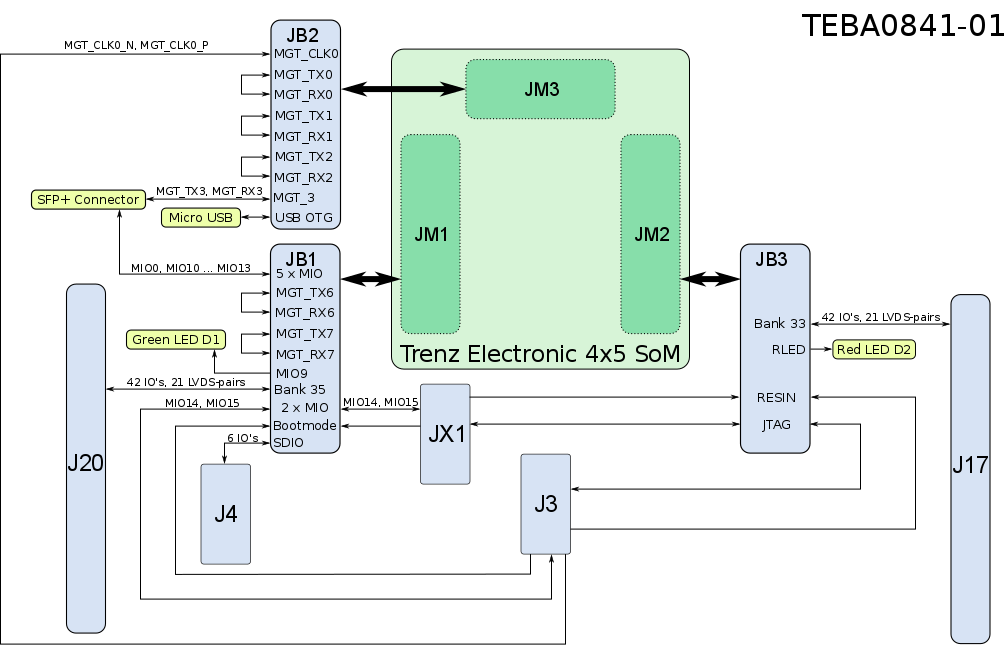
Figure 1: TEBA0841-01 Block Diagram
...
- Samtec Razor Beam™ LSHM-150 B2B connector JB1
- Samtec Razor Beam™ LSHM-150 B2B connector JB3
- Samtec Razor Beam™ LSHM-130 B2B connector JB2
- 6-pin header J26 for selecting VCCIOA supply-voltage
- 6-pin header J27 for selecting VCCIOD supply-voltage
- Micro USB Connector J12 (Device or OTG mode)
- JTAG header, connected to JTAG interface of 4 x 5 Module ('XMOD FTDI JTAG Adapter' compatible pin-assignment)
- User LED D1 (green)
- User LED D2 (red)
- SFP+ Connector J1
- 50-pin header soldering-pads J17 for access to SoM's IO-banks (LVDS-pairs possible)
- 50-pin header soldering-pads J20 for access to SoM's IO-banks (LVDS-pairs possible)
- 16-pin header soldering-pads J3, 'XMOD FTDI JTAG Adapter' compatible pin-assignment with 2 additional pins for reference-clock input to 4x5 SoM
- 10-pin header soldering-pads J4 for access to SoM's SDIO-port (voltage translation via SDIO Port Expander necessary)
...
| SFP+ pin | SFP+ pin netname | B2B | Note |
|---|---|---|---|
| Transmit Data + (pin 18) | MGT_TX3_P | JB2-26 | - |
| Transmit Data - (pin 19) | MGT_TX3_N | JB2-28 | - |
| Receive Data + (pin 13) | MGT_RX3_P | JB2-25 | - |
| Receive Data - (pin 12) | MGT_RX3_N | JB2-27 | - |
| Receive Fault (pin 2) | MIO10 | JB1-96 | - |
| Receive disable (pin 3) | not connected | - | - |
| MOD-DEF2 (pin 4) | MIO13 | JB1-98 | 3.3V pull-up, (SDA, I2C-Master) |
| MOD-DEF1 (pin 5) | MIO12 | JB1-100 | 3.3V pull-up, (SCL, I2C-Master) |
| MOD-DEF0 (pin 6) | MIO11 | JB1-94 | - |
| RS0 (pin 7) | not connected | - | - |
| LOS (pin 8) | MIO0 | JB1-88 | - |
| RS1 (pin 9) | not connected | - | - |
Table 1: SFP+ connector pin-assignment
Bridged MGT-Lanes on B2B Connector JB1 and JB2
The TEBA0841 Carrier Board is mainly for the 4 x 5 SoMs TE0841 and TE0741. This SoMs have GTX-Transceiver units on their FPGA-modules with up to 8 available MGT-lanes. To test this MGT-lanes, the 5 RX/TX differential pairs are bridged on-board, hence the transmitted data on this MGT-lanes are received simultaneously by the same MGT-lane.
The MGT-lane pins are bridged on-board as fellows, if 4 x 5 SoM TE0741 is mounted:
| MGT-lane | B2B TX diff-pair | B2B RX diff-pair | B2B-pins bridged |
|---|---|---|---|
| MGT-lane 0 | JB2-8 (MGT_TX0_N) JB2-10 (MGT_TX0_P) | JB2-7 (MGT_RX0_N) JB2-9 (MGT_RX0_P) | JB2-7 to JB2-8 |
JB2-9 to JB2-10 |
| MGT-lane 1 | JB2-14 (MGT_TX1_N) JB2-16 (MGT_TX1_P) | JB2-13 (MGT_RX1_N) JB2-15 (MGT_RX1_P) | JB2-13 to JB2-14 |
JB2-15 to JB2-16 |
| MGT-lane 2 |
JB2-20 (MGT_TX2_N) |
JB2-22 (MGT_TX2_P) |
JB2-19 (MGT_RX2_N) |
JB2-21 (MGT_RX2_P) |
JB2-19 to |
JB2-20 |
JB2-21 to |
JB2-22 |
| MGT-lane 7 | JB1-3 (MGT_TX7_P) JB1-5 (MGT_TX7_N) | JB1-9 (MGT_RX7_P) JB1-11 (MGT_RX7_N) | JB1-3 to JB1-9 |
JB1-5 to JB1-11 |
| MGT-lane 6 | JB1-15 (MGT_TX6_P) JB1-17 (MGT_TX6_N) | JB1-21 (MGT_RX6_P) JB1-23 (MGT_RX6_N) | JB1-15 to JB1-21 |
JB1-17 to JB1-23 |
Table 2: Bridging-table of the MGT-lanes for mounted 4 x 5 SoM TE0741.
| Note |
|---|
| Note: The MGT-lanes of the 4 x 5 SoM TE0841 have other designationsdifferent designations. See Schematic of the particular module. |
USB Interface
The TEBA0841 carrier board has one physical USB-connector J10, which is available as Micro-USB port. The USB interface J10 can be operated in Device- and OTG-modes. The Micro-USB port-pins are routed to the USB-OTG-interface on B2B-connector JB2. There are usually corresponding USB-PHYs on SoMs supported by the Carrier Board TEBA0841.
...
The JTAG-interface of the mounted 4 x 5 SoM can be accessed via header JX1. This header has a 'XMOD FTDI JTAG Adapter'-compatible pin-assignment.
| JX1 pin | JX1 pin net-name | B2B |
|---|---|---|
| C (pin 4) | TCK | JB3-100 |
| D (pin 8) | TDO | JB3-98 |
| F (pin 10) | TDI | JB3-96 |
| H (pin 12) | TMS | JB3-94 |
| A (pin 3) | MIO15 | JB1-86 |
| B (pin 7) | MIO14 | JB1-91 |
| E (pin 9) | BOOTMODE | JB1-90 (JTAGSELECT) |
| G (pin 11) | RESIN | JB3-17 |
Table 3: JTAG header JX1 pin-assignment
...
The PL IO-bank supply-voltages 1.8V, 2.5V and 3.3V will be available after the mounted module's 3.3V voltage level is present on B2B connector JM2 pins 10 and 12, meaning that all on-module voltages have become stable and module is properly powered up.
Note: The suppysupply-voltages have low current dropout.
Figure 3: Power-Up On sequence diagram
Configuring VCCIO
...
On the TEBA0841 carrier board the PL IO-bank's supply voltages of the 4x5 SoM (VCCIOA, VCCIOD; see 4x5 Module Integration Guide) are connected to the base-board VCCIO-voltage VCCIOA and VCCIOA VCCIOD, which are selectable between the supply-voltages 1.8V, 2.5V and 3.3V via jumper J26 and J27.
baseboard supply-voltages | base-board B2B connector-pins |
|---|
| standard assignment of PL IO-bank supply-voltages on TE 4x5 module's B2B connectors-pins | ||
|---|---|---|
| VCCIOA | JB1-10, JB1-12 | VCCIOA (JM1-9, JM1-11) |
| VCCIOD | JB2-8, JB2-10 | VCCIOD (JM2-7, JM2-9) |
Table 45: base-board supply-voltages VCCIOA and VCCIOD
| Note |
|---|
Note: The corresponding PL IO-voltage supply voltages of the 4x5 SoM to the selectable base-board voltage VIOTB VCCIOA and VCCIOD are depending on the mounted 4x5 SoM and varying in order of the used model. Refer to SoM's schematic to get information about the specific pin-assignment on module's B2B-connectors regarding PL IO-bank supply-voltages and to the 4x5 Module integration Guide for VCCIO voltage options. |
Following table describes how to configure the base-board supply-voltages by jumpers:
base-board supply-voltages vs voltage-levels | VCCIOA | VCCIOD |
|---|---|---|
| 1.8V | J26:1-2 | J27:1-2 |
| 2.5V | J26:3-4 | J27:3-4 |
| 3.3V | J26:5-6 | J27:5-6 |
Table 56: Configuration of base-board supply-voltages via jumpers. Jumper-Notification: 'Jx: 1-2' means pins 1 and 2 are connected, 'Jx: 3-4' means pins 3 and 4 are connected, and so on.
| Note |
|---|
| It is recommended to set and measure the PL IO-bank supply-voltages before mounting of TE 4x5 module to avoid failures and damages to the functionality of the mounted SoM. |
...
Physical Dimensions
Board size: PCB 17056.4 47 mm × 98 75 mm. Notice that some parts the are hanging slightly over the edge of the PCB like the mini USB-jacks (ca. 1.4 mm) and the Ethernet RJ-45 jack (ca 2.2 mm)and the SFP+ connector, which determine the total physical dimensions of the carrier board. Please download the assembly diagram for exact numbers.
Mating height of the module with standard connectors: 8mm
PCB thickness: ca. 1.65mm
Highest part on the PCB is the SFP+ connector, which has an approximately 17 11.3 mm overall hight. Please download the step model for exact numbers.
All The dimensions are given in mm and mil (milli inch).
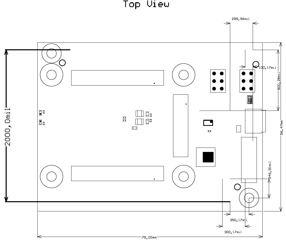
Figure 4: Physical Dimensions of the TE0705TEBA0841-04 01 carrier board
Operating Temperature Ranges
...
Board operating temperature range depends also on customer design and cooling solution. Please contact us for options.
Weight
ca. 110 32 g - Plain board
Document Change History
| date | revision | authors | description |
|---|---|---|---|
| 2017-02-1008 | Ali Naseri | current TRM for TEBA0841-01 | |
| 2017-01-30 | 0.1 | Ali Naseri | Initial document |
...
| Date | Revision | Notes | PCN | Documentation link |
|---|---|---|---|---|
| - | 01 |
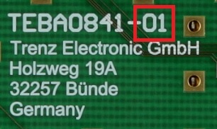
Figure 5: Hardware revision Number
...
Overview
Content Tools