Page History
...
| Scroll Only (inline) |
|---|
Refer to https://shop.trenz-electronic.de/de/Download/?path=Trenz_Electronic/carrier_boards/TEBA0841 for downloadable version of this manual and additional technical documentation of the product. |
The Trenz Electronic TEBA0841 Carrier Board is a base-board for 4 x 5 SoMs, which is dedicated to test- and evaluation-purposes of , especially for the Multi-gigabit transceiver units of Trenz Electronic 4x5 SoMsthe TE0841 and TE0741 modules. Although this base-board is dedicated to these modules, it is also compatible with other Trenz Electronic 4 x 5 cm SoMs. See page "4 x 5 cm carriers" to get information about the SoMs supported by the TEBA0841 base-board.
This base-board provides also soldering-pads as place-holders for pin-headers as option to get access to the PS- and PL-IO-banks of the mounted SoM.
See page "4 x 5 cm carriers" to get information about the SoMs supported by the TEBA0841 Carrier Board.
Block Diagram
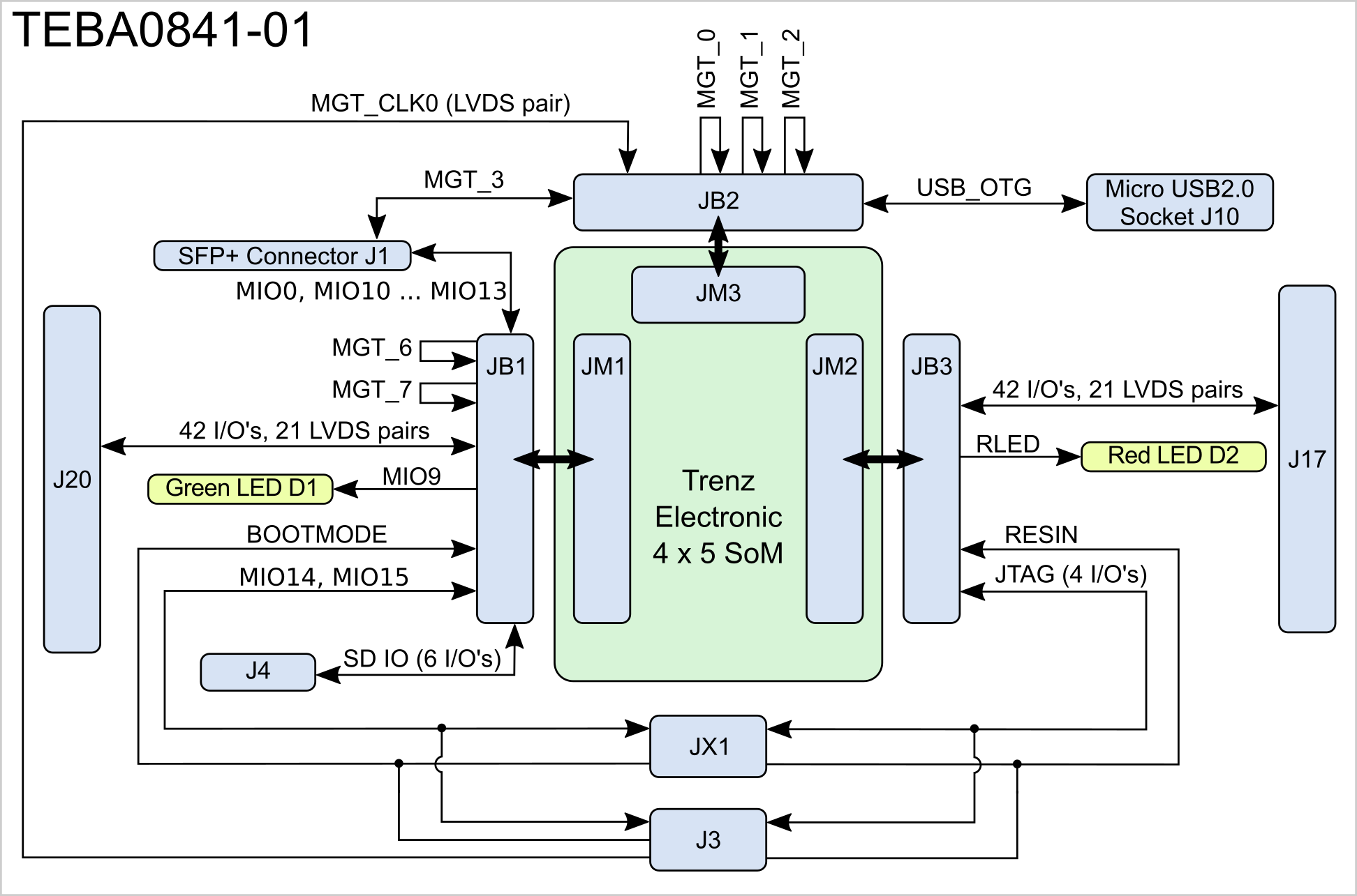
Figure 1: TEBA0841-01 Block Diagram
...
- Samtec Razor Beam™ LSHM-150 B2B connector JB1
- Samtec Razor Beam™ LSHM-150 B2B connector JB3
- Samtec Razor Beam™ LSHM-130 B2B connector JB2
- 6-pin header J26 for selecting VCCIOA PL IO-bank supply-voltage VCCIOA
- 6-pin header J27 for selecting VCCIOD PL IO-bank supply-voltage VCCIOD
- Micro USB Connector J12 (Device or OTG mode)
- JTAG header, connected to JTAG interface of 4 x 5 Module (/UART header with 'XMOD FTDI JTAG Adapter'-compatible pin-assignment)
- User LED D1 (green)
- User LED D2 (red)
- SFP+ Connector J1
- 50-pin header soldering-pads J17 for access to SoM's IO-banks (LVDS-pairs possible)
- 50-pin header soldering-pads J20 for access to SoM's IO-banks (LVDS-pairs possible)
- 16-pin header soldering-pads J3, 'XMOD FTDI JTAG Adapter'-compatible pin-assignment with 2 additional pins for reference-clock input to 4x5 SoM
- 10-pin header soldering-pads J4 for access to SoM's SDIO-port (voltage translation via SDIO Port Expander necessary), if available
Key Features
- SFP+ connector (Enhanced small form-factor pluggable), supports data transmission rates up to 10 Gbit/s
- Micro-USB-Interface (J10) connected to Zynq-module (Device or OTG mode)
- Trenz 4x5 module Socket (3 x Samtec LSHM series connectors)
- 4x5 SoM programable by JTAG header (JX1)
- 2 x user LEDs routed to MIOIO-pins of the SoM
- Soldering-pads J17 and J20 as place-holder for further possibilities to access to SoMs IO-bank-pins, usable as LVDS-pairs
- Soldering-pads J3 and J4 as place-holder for access to JTAG/UART- or SDIO-port of the SoM
...
The RX-/TX-data-lanes are connected to B2B-connector JB2, the control-lines are connected to to module's IO-pins on B2B-connector JB1 and are MIO(MIO0-bank-pins in standard TE module's pin-assignment).
On this SFP+ connector, on both 4 x 5 SoMs TE0741 and TE0841 MGT-lane 3 is accessible.
...
| SFP+ pin | SFP+ pin netname | B2B | Note |
|---|---|---|---|
| Transmit Data + (pin 18) | MGT_TX3_P | JB2-26 | - |
| Transmit Data - (pin 19) | MGT_TX3_N | JB2-28 | - |
| Receive Data + (pin 13) | MGT_RX3_P | JB2-25 | - |
| Receive Data - (pin 12) | MGT_RX3_N | JB2-27 | - |
| Receive Fault (pin 2) | MIO10 | JB1-96 | - |
| Receive disable (pin 3) | not connected | - | - |
| MOD-DEF2 (pin 4) | MIO13 | JB1-98 | 3.3V pull-up, (usuable as SDA, I²C-Master) |
| MOD-DEF1 (pin 5) | MIO12 | JB1-100 | 3.3V pull-up, (usuable as SCL, I²C-Master) |
| MOD-DEF0 (pin 6) | MIO11 | JB1-94 | - |
| RS0 (pin 7) | not connected | - | - |
| LOS (pin 8) | MIO0 | JB1-88 | - |
| RS1 (pin 9) | not connected | - | - |
...
The TEBA0841 Carrier Board is mainly for the 4 x 5 SoMs TE0841 and TE0741. This SoMs have GTX-Transceiver units on their FPGA-modules with up to 8 available MGT-lanes. To test this MGT-lanes, the 5 RX/TX differential pairs are bridged on-board, hence the transmitted data on this MGT-lanes are received simultaneously by the same MGT-lane in a loop-back circuit..
The MGT-lane pins are bridged on-board as fellows, if 4 x 5 SoM TE0741 is mounted:
...
The TEBA0841 carrier board has one physical USB-connector J10, which is available as Micro-USB port. The USB interface J10 can be operated in Device- and OTG-modes. The Micro-USB port-pins are routed to the USB-OTG-interface on B2B-connector JB2. There are usually corresponding USB-PHYs on SoMs supported by the Carrier Board TEBA0841.
JTAG/UART Interface
The JTAG-interface of the mounted 4 x 5 SoM can be accessed via header JX1. This header has a 'XMOD FTDI JTAG Adapter'-compatible pin-assignment.
| JX1 pin | JX1 pin net-name | B2B |
|---|---|---|
| C (pin 4) | TCK | JB3-100 |
| D (pin 8) | TDO | JB3-98 |
| F (pin 10) | TDI | JB3-96 |
| H (pin 12) | TMS | JB3-94 |
| A (pin 3) | MIO15 |
| JB1-86 (usable as UART-RX/TX) | ||
| B (pin 7) | MIO14 | JB1-91 (usable as UART-RX/TX) |
| E (pin 9) | BOOTMODE | JB1-90 (JTAGSELECT) |
| G (pin 11) | RESIN | JB3-17 |
Table 3: JTAG header JX1 pin-assignment
There is also the option to mount and solder a 2-row 16-pin header to the place-holder J3, which has the same pin-assignment as header JX1, but with also two additional pins (15,16) as LVDS-pair, to put an external reference clock-signal to the mounted 4 x 5 SoM. The clock-signal is put to to the SoM via B2B-connector pins JB2-32 (MGT_CLK0_N, J3-16) and JB2-34 (MGT_CLK0_P, J3-15).
On both interfaces (JX1, J3), the pins with the net-names MIO14 and MIO15 are available as user IO's which could be used as UART-interface for example.
...
There are two LEDs D1 (green) and D2 (red) available to the user. The green LED D1 is connected to the pin MIO9 ( JB1-92 )with the net-name 'MIO9', the red LED D2 is connected to the pin JB3-90 with the net-name 'RLED'.
Header place-holder J4
The place-holder J4 with solder-pads to mount a 2-row 10-pin header provides the capability, to access via this header the SDIO-port of the mounted 4 x 5 SoM, if available. For this purpose, there is also voltage-translation via SDIO port expander (e.g. Texas Instruments TXS02612) necessary due to the different voltage levels of the Micro SD Card (3.3V) and MIO MIO0-bank of the Xilinx Zynq-chip (1.8V).
In other cases this can be used to access PL IO-bank-pins of the SoM.
Header place-holder J17 and J20
...
Overview
Content Tools