Page History
...
Main Components
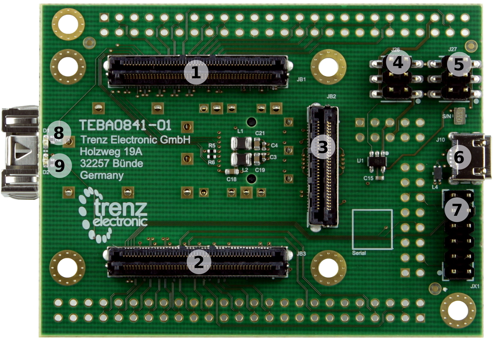
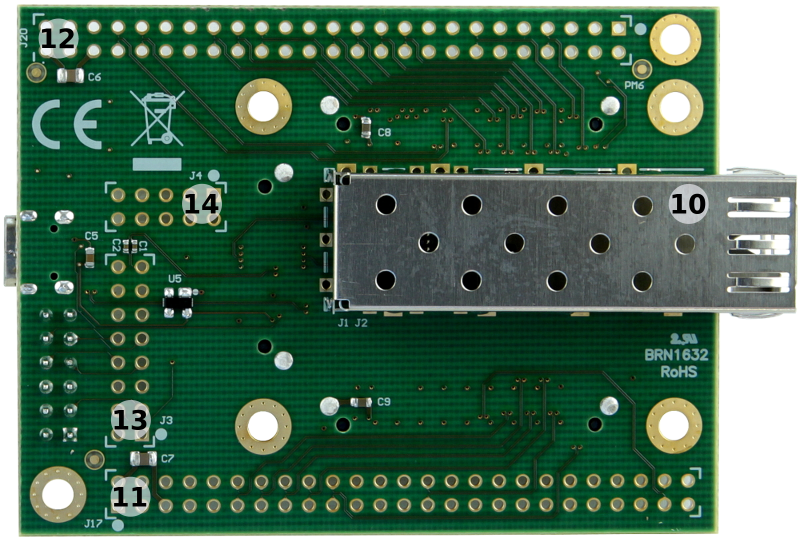
Figure 2: 4x5 4 x 5 SoM carrier board TEBA0841-01
...
- Samtec Razor Beam™ LSHM-150 B2B connector JB1
- Samtec Razor Beam™ LSHM-150 B2B connector JB3
- Samtec Razor Beam™ LSHM-130 B2B connector JB2
- 6-pin header J26 for selecting PL IO-bank supply-voltage VCCIOA
- 6-pin header J27 for selecting PL IO-bank supply-voltage VCCIOD
- Micro USB Connector J12 (Device or OTG mode)
- JTAG/UART header with 'XMOD FTDI JTAG Adapter'-compatible pin-assignment
- User LED D1 (green)
- User LED D2 (red)
- SFP+ Connector J1
- 50-pin header soldering-pads J17 for access to SoM's IO-banks (LVDS-pairs possible)
- 50-pin header soldering-pads J20 for access to SoM's IO-banks (LVDS-pairs possible)
- 16-pin header soldering-pads J3, 'XMOD FTDI JTAG Adapter'-compatible pin-assignment with 2 additional pins for reference-clock input to 4x5 4 x 5 SoM
- 10-pin header soldering-pads J4 for access to SoM's SDIO-port, if available
...
| SFP+ pin | SFP+ pin netname | B2B | Note |
|---|---|---|---|
| Transmit Data + (pin 18) | MGT_TX3_P | JB2-26 | - |
| Transmit Data - (pin 19) | MGT_TX3_N | JB2-28 | - |
| Receive Data + (pin 13) | MGT_RX3_P | JB2-25 | - |
| Receive Data - (pin 12) | MGT_RX3_N | JB2-27 | - |
| Receive Fault (pin 2) | MIO10 | JB1-96 | - |
| Receive disable (pin 3) | not connected | - | - |
| MOD-DEF2 (pin 4) | MIO13 | JB1-98 | 3.3V pull-up, (usuable as SDA, I²C-Masterusable I²C SDA/SCL-line) |
| MOD-DEF1 (pin 5) | MIO12 | JB1-100 | 3.3V pull-up, (usuable as SCL, I²C-Masterusable I²C SDA/SCL-line) |
| MOD-DEF0 (pin 6) | MIO11 | JB1-94 | - |
| RS0 (pin 7) | not connected | - | - |
| LOS (pin 8) | MIO0 | JB1-88 | - |
| RS1 (pin 9) | not connected | - | - |
Table 1: SFP+ connector pin-assignment
...
Looped-backed MGT-Lanes on B2B Connector JB1 and JB2
The TEBA0841 Carrier Board is mainly for the 4 x 5 SoMs TE0841 and TE0741. This SoMs have GTX-Transceiver units on their FPGA-modules with up to 8 available MGT-lanes. To test this MGT-lanes, the 5 RX/TX differential pairs are bridged on-board, hence the transmitted data on this MGT-lanes are received simultaneously by the same MGT-lane lanes flows back to their source in a loop-back circuit without intentional processing or modification..
The MGT-lane pins are bridged on-board as fellows, if 4 x 5 SoM TE0741 is mounted on carrier board:
| MGT-lane | B2B TX diff-pair | B2B RX diff-pair | B2B-pins bridged |
|---|---|---|---|
| MGT-lane 0 | JB2-8 (MGT_TX0_N) JB2-10 (MGT_TX0_P) | JB2-7 (MGT_RX0_N) JB2-9 (MGT_RX0_P) | JB2-7 to JB2-8 JB2-9 to JB2-10 |
| MGT-lane 1 | JB2-14 (MGT_TX1_N) JB2-16 (MGT_TX1_P) | JB2-13 (MGT_RX1_N) JB2-15 (MGT_RX1_P) | JB2-13 to JB2-14 JB2-15 to JB2-16 |
| MGT-lane 2 | JB2-20 (MGT_TX2_N) JB2-22 (MGT_TX2_P) | JB2-19 (MGT_RX2_N) JB2-21 (MGT_RX2_P) | JB2-19 to JB2-20 JB2-21 to JB2-22 |
| MGT-lane 7 | JB1-3 (MGT_TX7_P) JB1-5 (MGT_TX7_N) | JB1-9 (MGT_RX7_P) JB1-11 (MGT_RX7_N) | JB1-3 to JB1-9 JB1-5 to JB1-11 |
| MGT-lane 6 | JB1-15 (MGT_TX6_P) JB1-17 (MGT_TX6_N) | JB1-21 (MGT_RX6_P) JB1-23 (MGT_RX6_N) | JB1-15 to JB1-21 JB1-17 to JB1-23 |
Table 2: BridgingLooped-table of the backed MGT-lanes for mounted 4 x 5 SoM TE0741.
...
The JTAG-interface of the mounted 4 x 5 SoM can be accessed via header JX1. This header has a 'XMOD FTDI JTAG Adapter'-compatible pin-assignment.
| JX1 pin | JX1 pin net-name | B2B |
|---|---|---|
| C (pin 4) | TCK | JB3-100 |
| D (pin 8) | TDO | JB3-98 |
| F (pin 10) | TDI | JB3-96 |
| H (pin 12) | TMS | JB3-94 |
| A (pin 3) | MIO15 | JB1-86 (usable as UART |
| RX/TX-line) | ||
| B (pin 7) | MIO14 | JB1-91 (usable as UART |
| RX/TX-line) | ||
| E (pin 9) | BOOTMODE | JB1-90 (JTAGSELECT) |
| G (pin 11) | RESIN | JB3-17 |
Table 3: JTAG header JX1 pin-assignment
There is also the option to mount and solder a 2-row 16-pin header to the place-holder J3, which has the same pin-assignment as header JX1, but with also two additional pins (15,16) as LVDS-pair , to put an external reference clock-signal to the mounted 4 x 5 SoM. The clock-signal is put to to the SoM via B2B-connector pins JB2-32 (MGT_CLK0_N, J3-16) and JB2-34 (MGT_CLK0_P, J3-15).
...
The place-holder J4 with solder-pads to mount a 2-row 10-pin header provides the capability, to access via this header the SDIO-port of the mounted 4 x 5 SoM, if available. For this purpose, there is also voltage-translation via SDIO port expander (e.g. Texas Instruments TXS02612) necessary due to the different voltage levels of the Micro SD Card (3.3V) and MIO0-bank of the Xilinx Zynq-chip (1.8V).
In other cases this the connector J4 can be used to access the PL IO-bank-pins of the SoM.
...
The external power-supply can be connected to the board by the following pins:
| Connector | 3.3V pin | GND pin |
|---|---|---|
| JX1 | JX1-5, JX1-6, | JX1-1, JX1-2 |
| J3 | J3-5, J3-6 | J3-1, J3-2 |
| J4 | J4-5 | J4-1, J4-2 |
| J20 | J20-5, J20-46 | J20-1 , J20-2 , J20-49 , J20-50 |
| J17 | J17-5, J17-46 | J17-1 , J17-2 , J17-49 , J17-50 |
Table 4: Connector-pins capable for external 3.3V power-supply
...
The PL IO-bank supply-voltages 1.8V, 2.5V and 3.3V will be available after the mounted module's 3.3V voltage level is present on B2B connector JM2 pins 10 and 12, meaning that all on-module voltages have become stable and module is properly powered up.
Note: The DCDC-converters generating the supply-voltages have low current dropout.
...
| date | revision | authors | description |
|---|---|---|---|
| 2017-02-0815 | Ali Naseri | current TRM for TEBA0841-01 | |
| 2017-01-30 | 0.1 | Ali Naseri | Initial document |
...
Overview
Content Tools