Page History
...
| Scroll pdf ignore | |
|---|---|
Table of Contents
|
Overview
| Scroll Only (inline) |
|---|
Refer to https:// |
...
wiki.trenz-electronic.de/ |
...
display/ |
...
PD/TE0726+TRM for |
...
online version of this manual and additional technical documentation of the product. |
The Trenz Electronic TE0726 "ZynqBerry" is a industrial-grade Raspberry Pi form-factor compatible FPGA SoM (System on Module) based on Xilinx Zynq-7010 SoC (XC7Z010 System on Chip) with up to 512 MByte DDR3L SDRAM, 4 x USB 2.0 ports, 10/100 Mbit Ethernet port and 16 MByte Flash memory.
...
- Xilinx Zynq XC7Z010-1CLG225C
- REV3: DDR3L SDRAM (512MByte512 MByte)
- REV2: DDR3L SDRAM (128 - 512 MByte)
- REV1: LPDDR2 SDRAM (64 MByte) - 16 MByte Flash
- Raspberry Pi Model 2 form factor
- LAN9514 USB hub with 10/100 Ethernet
- 4 x USB 2.0 with power switches
- 10/100 Mbit Ethernet RJ45 - Micro SD card slot with card-detect switch
- HDMI connector
- DSI connector (Display)
- CSI-2 connector (Camera)
- HAT header with 26 I/Os
- Micro-USB
- power input
- USB UART
- JTAG ARM- and FPGA-Debug - 3.5 mm stereo audio socket (PWM audio output only)
Page break
Block Diagram
...
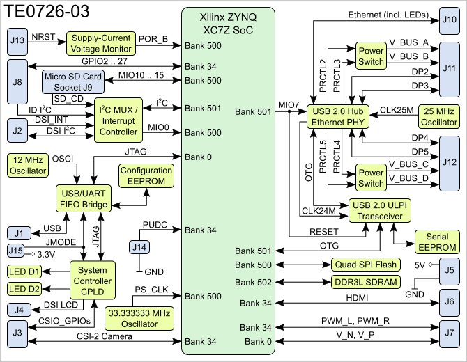
Main Components
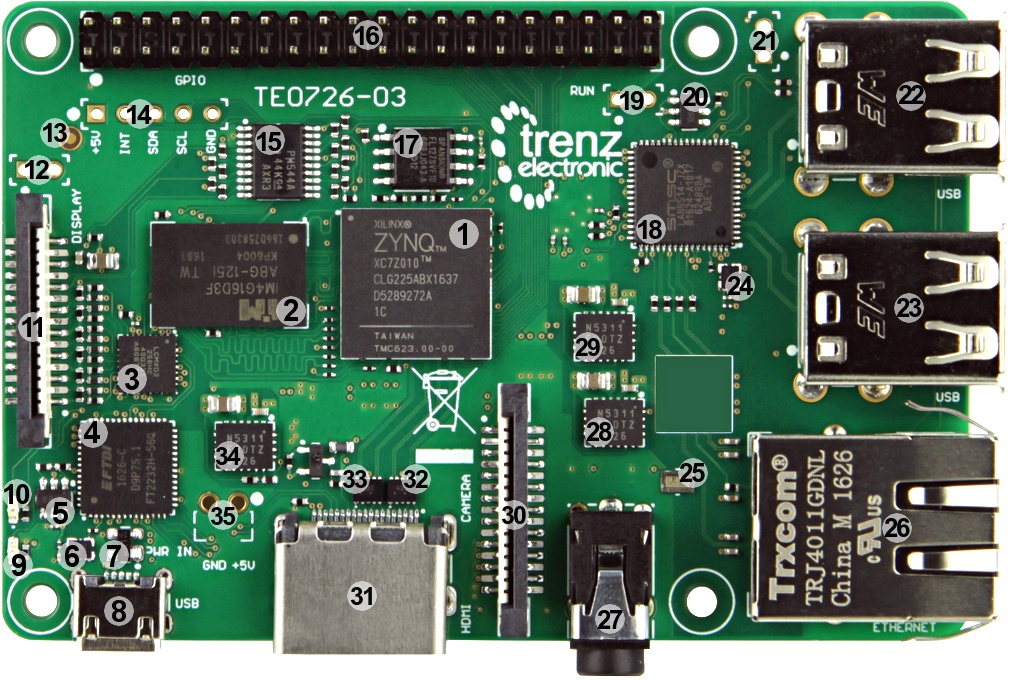
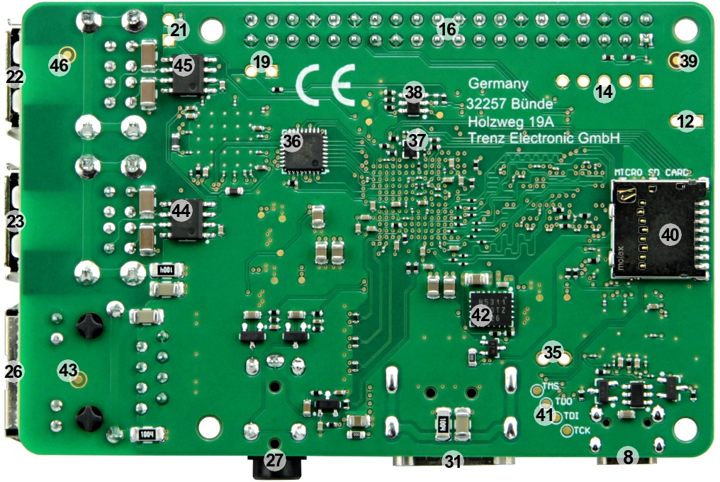
- Xilinx Zynq XC7Z010 All Programmable SoC, U1
- 512 MByte DDR3L SDRAM, U8
- Lattice Semiconductor MachXO2 System Controller CPLD, U11
- Dual high-speed USB to multipurpose UART/FIFO, U3
- 2 Kbit Microwire compatible serial EEPROM, U6
- Low-power, programmable oscillator @ 12.000000 MHz, U7
- Ultra-low capacitance double rail-to-rail ESD protection diode ,U4
- Micro-USB 2.0 B receptacle, J1
- Green LED (GLED), D1
- Red LED (RLED), D2
- DSI LCD connector, J4
- JTAGENB, when low, TDO, TDI, TMS and TCK function as GPIOs, J15
- Fiducial mark PM2
- External I2C bus with interrupt signal and power line, J2
- Low-voltage 4-channel I2C and SMBus multiplexer with interrupt logic, U10
- 2x20 pin 2.54 GPIO header, J8
128 Mbit (16 MByte) 3.0V SPI Flash memory, U5
- USB 2.0 Hub and 10/100 Ethernet controller, U2
- External reset
- 2 Kbit Microwire compatible serial EEPROM, U9
- PUDC of Zynq, active low enables internal pull-ups during configuration on all SelectIO pins
- Dual USB A receptacle, J12. Also fiducial mark PM1
- Dual USB A receptacle, J11
- Low power programmable oscillator @ 25.000000 MHz, U13
- Molex’s miniature traceability S/N pad for low-cost, unique product identification
- RJ-45 Ethernet connector with 10/100 integrated magnetics, J10. Also fiducial mark PM3
- 3.5mm RCA audio jack, J7
- 1A PowerSoC synchronous buck regulator with integrated inductor (3.3V), U20
- 1A PowerSoC synchronous buck regulator with integrated inductor (1.8V), U19
- ZIF FFC/FPC CSI-2 camera connector, J3
- HDMI connector, J6
Common mode filter with ESD protection, D8
Common mode filter with ESD protection, D9
- 1A PowerSoC synchronous buck regulator with integrated inductor (1.35V), U16
- Additional external +5V power supply connector, J5
Highly integrated full featured hi-speed USB 2.0 ULPI transceiver, U18
- Low-power programmable oscillator @ 33.333333 MHz, U14
- Ultra-low supply current voltage monitor with optional watchdog, U22
- Fiducial mark PM4
- Micro SD memory card connector with detect switch, J9
- JTAG interface, TP1 (TDI), TP3 (TDO), TP5 (TCK), TP7 (TMS)
- 1A PowerSoC synchronous buck regulator with integrated inductor (1.0V), U17
- Fiducial mark PM6
- 0.5A dual channel current-limited power switch, U15
- 0.5A dual channel current-limited power switch, U21
- Fiducial mark PM5
...
| Bank | Zynq Pin | Name | Connected To |
|---|---|---|---|
| 34 | G14 | PUDC | Jumper J14 |
| 35 | G15 | DSI_XA | System Controller CPLD, pin 16 |
| 35 | F15 | DSI_XB | System Controller CPLD, pin 17 |
...
Header J8 Interface Mapping
...
26 PL IO and 2 MIO IOs over I2C mux. All Bank IO voltages are 3.3V.
| J8 Pin |
|---|
| Name |
|---|
| Zynq Pin | Zynq Pin | Name | J8 Pin |
|---|
| 1 | 3.3V |
| - | - | 5V | 2 | |||
| 3 | GPIO2 | K15 | - | 5V | 4 | |
| 5 |
| GPIO3 | J14 |
| - |
| GND |
| 6 |
| 7 | GPIO4 | H12 | M12 | GPIO14 |
| 8 |
| 9 |
| GND |
| - |
| N13 |
| GPIO15 |
| 10 |
| 11 |
| GPIO17 |
| G11 | H11 | GPIO18 | 12 |
| 13 |
| GPIO27 |
| G12 |
| - |
| GND |
| 14 |
| 15 |
| GPIO22 |
| H13 |
| J11 |
| GPIO23 |
| 16 |
| 17 |
| 3.3V |
| - |
| K11 |
| GPIO24 |
| 18 |
| 19 |
| GPIO10 |
| H14 |
| - |
| GND |
| 20 |
| 21 |
| GPIO9 |
| J13 |
| K13 |
| GPIO25 |
| 22 |
| 23 |
| GPIO11 |
| J15 |
| L15 |
| GPIO8 |
| 24 |
| 25 |
| GND |
| - |
| L14 |
| GPIO7 |
| 26 |
| Page break |
|---|
| 27 | MIO49(ID_SDA via TCA9544APWR) | MIO48 (ID_SCL via TCA9544APWR ) | 28 | |||
| 29 | GPIO5 | N14 | - | GND | 30 | |
| 31 | GPIO6 | R15 | M15 | GPIO12 | 32 | |
| 33 | GPIO13 | R13 | - | GND | 34 | |
| 35 | GPIO19 | R12 | L13 | GPIO16 | 36 | |
| 37 | GPIO26 | L12 | M14 | GPIO20 | 38 | |
| 39 | GND | - | P15 | GPIO21 | 40 |
Page break
Default MIO Mapping
Bank 500 MIOs
...
| MIO | Function | Notes |
|---|---|---|
| 28 | OTG-DATA4 | ULPI bi-directional data bus. |
| 29 | OTG-DIR | Data bus direction control signal. |
| 30 | OTG-STP | Data throttle signal. |
| 31 | OTG-NXT | Data stream stop. |
| 32 | OTG-DATA0 | ULPI bi-directional data bus. |
| 33 | OTG-DATA1 | ULPI bi-directional data bus. |
| 34 | OTG-DATA2 | ULPI bi-directional data bus. |
| 35 | OTG-DATA3 | ULPI bi-directional data bus. |
| 36 | OTG-CLK | ULPI clock. |
| 37 | OTG-DATA5 | ULPI bi-directional data bus. |
| 38 | OTG-DATA6 | ULPI bi-directional data bus. |
| 39 | OTG-DATA7 | ULPI bi-directional data bus. |
| 48 | MUX_SCL | I2C clock to I2C MUX. |
| 49 | MUX_SDA | I2C data to/from I2C MUX. |
| 52 | MIO52 | System Controller CPLD pin 20 |
| 53 | MIO53 | System Controller CPLD pin 21 |
...
On-board LEDs
There are two LEDs on TE0726 module:
...
There is a System Controller CPLD chip LCMXO2-256HC from Lattice Semiconductor on-board. Refer to the TE0726 CPLD for more information.
Clocking
...
Signal Name
...
Default Frequency
...
Destination IC
...
Pin
...
Notes
...
33.333333 MHz
...
U1
...
C7
...
12.000000 MHz
...
U3
...
3
...
FT2232H oscillator input.
...
Hi-speed USB 2.0 and 10/100 Mbit Ethernet
The TE0726-03 has on-board SMSC LAN9514 controller featuring USB 2.0 hub and 10/100 Mbit Ethernet controller. USB hub has four downstream ports and one upstream port, fully compliant with Universal Serial Bus Specification Revision 2.0. HS (480 Mbps), FS (12 Mbps), and LS (1.5 Mbps) compatible. Upstream port is connected to the SMSC USB3320 hi-speed USB 2.0 ULPI transceiver which has full support for the optional On-The-Go (OTG) protocol.
High-Performance 10/100 Ethernet controller integrated into the same LAN9514 IC is fully compliant with IEEE802.3/802.3u standards, has integrated Ethernet MAC and PHY and supports both 10BASE-T and 100BASE-TX media.
256-byte EEPROM is connected via Microwire to the LAN9514 chip to store MAC address.
USB to JTAG/UART
The TE0726-03 has on-board high-speed USB 2.0 to UART/FIFO FT2232H controller from FTDI with external connection to micro-USB connector J1. There is also a 256-byte EEPROM wired to the FT2232H chip via Microwire bus which holds pre-programmed license code to support Xilinx programming tools.
| Warning |
|---|
Do not access the FT2232H EEPROM using FTDI programming tools, doing so will erase normally invisible user EEPROM content and invalidate stored Xilinx JTAG license. Without this license the on-board JTAG will not be accessible any more with any Xilinx tools. Software tools from FTDI website do not warn or ask for confirmation before erasing user EEPROM content. |
4-Channel I2C Multiplexer
Zynq MIO pin 48 (MUX_SCL) and pin 49 (MUX_SDA) are connected to the 4-channel I2C multiplexer chip TCA9544A from Texas Instruments having I2C address of 0x70. It has four slave I2C channels which are routed as follows:
...
Channel
...
Connected To
...
0
...
Connector J8, pin 27 (ID_SDA) and pin 28 (ID_SCL).
...
1
...
DSI connector J4, pin 12 (DSI_SDA) and pin 11 (DSI_SCL).
...
2
...
HDMI connector J6, pin 16 (SDA) and pin 15 (SCL).
...
3
...
CSI-2 camera connector J3, pin 14 (CSI_SDA) and pin 13 (CSI_SCL).
Quad SPI Flash Memory
On-board QSPI flash memory (U5) on the TE0726 is provided by Cypress Semiconductor Serial NOR Flash Memory S25FL127SABMFV10 with 128 Mbit (16 MByte) storage capacity connected to the PS MIO bank (MIO1 ... MIO6) of the Zynq SoC. This non volatile memory is used to store initial FPGA configuration. Besides FPGA configuration, remaining free flash memory can be used for user application and data storage. All four SPI data lines are connected to the Zynq PS MIO-bank allowing x1, x2 or x4 data bus widths. Maximum data rate depends on the selected bus width and clock frequency used.
DDR3L SDRAM
The TE0726 SoM is equipped with one DDR3L-1600 SDRAM module with 1 GByte memory density. The SDRAM module is connected to the Zynq SoC's PS DDR controller with 16-bit data bus-width.
Clocking
Signal Name | Clock IC | Default Frequency | Destination IC | Pin | Notes |
|---|---|---|---|---|---|
| PS_CLK | U14 | 33.333333 MHz | U1 | C7 | Zynq SoC system reference clock. |
| OSCI | U7 | 12.000000 MHz | U3 | 3 | FT2232H oscillator input. |
| CLK24M | U2 | 24 MHz (see also REFSEL0 .. 2) | U18 | 26 | Reference input/output clock, see datasheet. |
| CLK25M | U13 | 25.000000 MHz | U2 | 61 | External 25 MHz crystal input. |
Hi-speed USB 2.0 and 10/100 Mbit Ethernet
The TE0726-03 has on-board SMSC LAN9514 controller featuring USB 2.0 hub and 10/100 Mbit Ethernet controller. USB hub has four downstream ports and one upstream port, fully compliant with Universal Serial Bus Specification Revision 2.0. HS (480 Mbps), FS (12 Mbps), and LS (1.5 Mbps) compatible. Upstream port is connected to the SMSC USB3320 hi-speed USB 2.0 ULPI transceiver which has full support for the optional On-The-Go (OTG) protocol.
High-Performance 10/100 Ethernet controller integrated into the same LAN9514 IC is fully compliant with IEEE802.3/802.3u standards, has integrated Ethernet MAC and PHY and supports both 10BASE-T and 100BASE-TX media.
256-byte EEPROM is connected via Microwire to the LAN9514 chip to store MAC address.
USB to JTAG/UART
The TE0726-03 has on-board high-speed USB 2.0 to UART/FIFO FT2232H controller from FTDI with external connection to micro-USB connector J1. There is also a 256-byte EEPROM wired to the FT2232H chip via Microwire bus which holds pre-programmed license code to support Xilinx programming tools.
| Warning |
|---|
Do not access the FT2232H EEPROM using FTDI programming tools, doing so will erase normally invisible user EEPROM content and invalidate stored Xilinx JTAG license. Without this license the on-board JTAG will not be accessible any more with any Xilinx tools. Software tools from FTDI website do not warn or ask for confirmation before erasing user EEPROM content. |
4-Channel I2C Multiplexer
Zynq MIO pin 48 (MUX_SCL) and pin 49 (MUX_SDA) are connected to the 4-channel I2C multiplexer chip TCA9544A from Texas Instruments having I2C address of 0x70. It has four slave I2C channels which are routed as follows:
Channel | Connected To |
|---|---|
0 | Connector J8, pin 27 (ID_SDA) and pin 28 (ID_SCL). |
1 | DSI connector J4, pin 12 (DSI_SDA) and pin 11 (DSI_SCL). |
2 | HDMI connector J6, pin 16 (SDA) and pin 15 (SCL). |
3 | CSI-2 camera connector J3, pin 14 (CSI_SDA) and pin 13 (CSI_SCL). |
Each slave channel of TCA9544A has its own dedicated interrupt signal in order for the master to detect an interrupt on the INT output pin that can result from any of the slave devices connected to the INT0-INT3 input pins.
Boot Process
Xilinx Zynq devices in CLG225 package do not support SD Card boot directly from ROM bootloader.
At least FSBL must be loaded from on-board SPI Flash, later all boot process can continue from SD Card. The easiest solution is to let FSBL to load bitstream and u-boot from SPI Flash, and then let u-boot to load Linux or any other OS image from SD Card.
Power and Power-On Sequence
Power Consumption
TE0726 needs one single power source via Micro USB2.0 B socket J1. However, it is recommended to not use any USB equipment below USB standard 2.0 to power the module. Also two-pin header J5 can be used as alternative to feed the 5V power supply voltage.
The maximum power consumption of a module mainly depends on the design which is running on the FPGA.
Xilinx provide a power estimator excel sheets to calculate power consumption. It's also possible to evaluate the power consumption of the developed design with Vivado. See also Trenz Electronic Wiki FAQ.
Each slave channel of TCA9544A has its own dedicated interrupt signal in order for the master to detect an interrupt on the INT output pin that can result from any of the slave devices connected to the INT0-INT3 input pins.
Boot Process
Xilinx Zynq devices in CLG225 package do not support SD Card boot directly from ROM bootloader.
At least FSBL must be loaded from on-board SPI Flash, later all boot process can continue from SD Card. The easiest solution is to let FSBL to load bitstream and u-boot from SPI Flash, and then let u-boot to load Linux or any other OS image from SD Card.
Power and Power-On Sequence
To power-up a module, 5.0V power supply with minimum current capability of 1A is recommended.
Power Supply
TE0726 needs one single power source via micro-USB jack J1. However it is recommended to not use any USB equipment below USB standard 2.0 to power the module. Also two-pin header J5 can be used to provide power source if needed.
...
of 1A is recommended.
Power Distribution Dependencies
There is no specific power-on sequence, except to achieve minimum current draw, I/Os should be 3-stated at power-on.
There are following dependencies how the power supply voltage (5V nominal) is distributed to the on-board DC-DC converters.
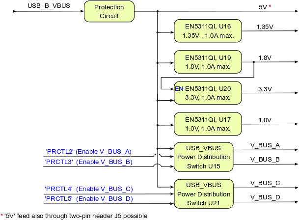
Power Rails and Bank Voltages
...
If TE0726 module is powered by micro-USB connector J1 VBUS pin, which voltage level is controlled by supplying host according to the USB standards and should be 5V, there is not much user can control here if using standard USB equipment. However, user can also power the module by applying voltage to the J5 connector from other external sources. In both cases following maximum voltage ratings apply.
Absolute Maximum Ratings
Parameter | Min | Max | Units | Notes |
|---|---|---|---|---|
Power supply voltage J1: USB_V_BUS |
, J5: 5V | 4.75 | 5.25 | V | - |
| VOUT of AP2152SG-13 | - | VIN + 0.3 | V | Output voltage. |
| ILOAD of AP2152SG-13 | - | Internal limited | A | Maximum continuous |
| load current. | ||||
| PS MIO supply voltage | -0.5 | 3.6 | V | See Xilinx DS187 datasheet |
| PS MIO input voltage | -0.4 | VCCO_MIO + 0.55 | V | VCCO_MIO0_500 and VCCO_MIO1_501. |
| PL |
| HR I/O |
| banks supply voltage | -0. |
| 5 | 3.6 |
| V |
| See Xilinx DS187 datasheet |
| PL |
| HR I/O banks input voltage | -0.4 | VCCO |
| + 0.55 | V |
| See Xilinx DS187 datasheet | ||||
Storage temperature | -55 | +125 | °C | - |
See also the Xilinx datasheet DS187 for more information about absolute maximum ratings.
Recommended Operating Conditions
| Parameter | Min | Max | Units | Notes |
|---|---|---|---|---|
Power supply voltage J1: USB_V_BUS, J5: 5V | 4.75 | 5.5 | V | See AP2152SG-13 datasheet. |
| IOUT of AP2152SG-13 | 0 | 500 |
| mA | - | |||
| PS MIO supply voltage | 1.71 | 3.465 | V | See Xilinx DS187 datasheet |
| PS MIO input voltage | -0.2 | VCCO_MIO + 0.2 | V | VCCO_MIO0_500 and VCCO_MIO1_501. |
| PL |
| HR I/O |
| banks supply voltage |
| 1. |
| 14 | 3.465 |
| V |
| See Xilinx DS187 datasheet |
| PL |
| HR I/O banks input voltage | -0.2 | VCCO |
| + 0.2 | V |
| See Xilinx DS187 datasheet | ||||
| Operating temperature | 0 | 70 | °C | See LAN9514 datasheet. |
The module operating temperature range depends on customer design and cooling solution. Please contact us for options.
Page break
Physical Dimensions
Module size: 40 mm × 30 mm. Please download the assembly diagram for exact numbers.
Mating height with standard connectors: 8 mm
PCB thickness: 1.6 mm
Highest part on PCB: approximately 2.5 mm. Please download the step model for exact numbers.
...
Hardware revision number is printed on the PCB board next to the module model number separated by the dash.

Document Change History
.
Document Change History
Date | Revision | Contributors | Description | ||||
|---|---|---|---|---|---|---|---|
| 2017-11-10 | John Hartfiel |
| |||||
| 2017-11-10 | v.51 | Ali Naseri |
| Date | Revision | Contributors | Description|
| 2017-05-2430 | v.40 | Jan Kumann |
| 2017-05-24 | V.2 | John Hartfiel |
|
2017-05-24 | V.1V1 | Jan Kumann |
|
Disclaimer
| Include Page | ||||
|---|---|---|---|---|
|
Overview
Content Tools