Page History
...
| HTML |
|---|
<!-- General Notes: Designate all graphics and pictures with a number and a description. For example "Figure 1: TE07xx-xx Block Diagram" or "Table 1: Initial delivery state". "Figure x" and "Table x" have to be formatted to bold. --> |
| Scroll Ignore |
|---|
Download PDF version of this document. |
| Scroll pdf ignore | |
|---|---|
Table of Contents
|
...
| Scroll Only (inline) |
|---|
Refer to https://shopwiki.trenz-electronic.de/de/Download/?path=Trenz_Electronic/XMODdisplay/PD/TE0791+TRM for downloadablethe current online version of this manual and additionalother technicalavailable documentation of the product. |
The Trenz Electronic TE0791-01 is an adapter board for use with the XMOD TE0790 board. The adapter board provides several connector types to get access to the signals and interfaces of the XMOD board. As further option footprints are available for JST Wire-To-Board IDC connectors with two different pin-assignments.
...
Signals, Interfaces and Pins
Top View |
Bottom View flipped |
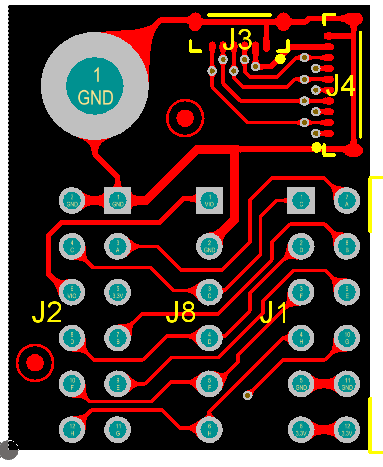
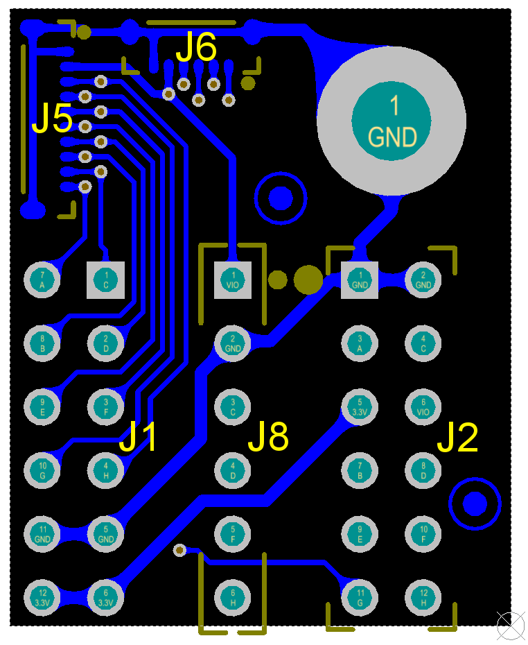
Figure 3: Connector Location
2x6 Pin Header
The 2x6 pin header (2.54mm grid size, male) J2 of the TE0791 board have to be connected to the corresponding XMOD pin header on the TE0790 board. The signal assignment of the pin header on the TE0790 board depends on the configuration of its System Controller CPLD firmware.
...
| J8 Pin Number | J8 Pin Name | Signal | Note |
|---|---|---|---|
| 1 | VIO | VCCIO | depends on TE0790 voltage check TE0790 DIP-switch settings |
| 2 | GND | Ground | - |
| 3 | C | TCK | - |
| 4 | D | TDO | - |
| 5 | F | TDI | - |
| 6 | H | TMS | - |
...
| Note | Signal | J1 Pin Name | J1 Pin Number | J1 Pin Number | J1 Pin Name | Signal | Note |
|---|---|---|---|---|---|---|---|
| - | UART TXD | A | 7 | 1 | C | TCK | - |
- | UART RXD | B | 8 | 2 | D | TDO | - |
| usable as GPIO | LED on TE0790 | E | 9 | 3 | F | TDI | - |
| usable as GPIO | Button on TE0790 | G | 10 | 4 | H | TMS | - |
| - | Ground | GND | 11 | 5 | GND | Ground | - |
| check TE0790 DIP-switch settings | VCC / VCCIO | 3.3V | 12 | 6 | 3.3V | VCC / VCCIO | check TE0790 DIP-switch settings |
Table 3: PMOD J1 signal assignment with standard TE0790 CPLD firmware
...
On the TE0791 board are footprints available for 10-pin JST Wire-To-Board IDC connectors J4 and J5 with two different pin-assignments, where all XMOD signals A - H are available. The pin- and signal-assignment with standard System Controller CPLD firmware of the XMOD board are as follows:
| Pin Name | J4 Pin Number | J5 Pin Number | Signal | Note |
|---|---|---|---|---|
| A | 1 | 10 | UART TXD | |
| B | 3 | 8 | UART RXD | - |
| C | 2 | 9 | TCK | - |
| D | 4 | 7 | TDO | - |
| E | 5 | 6 | LED on TE0790 | usable as GPIO |
| F | 6 | 5 | TDI | - |
| G | 7 | 4 | Button on TE0790 | usable as GPIO |
| H | 8 | 3 | TMS | - |
| VIO | 9 | 2 | VCC / VCCIO | check TE0790 DIP-switch settings |
| GND | 10 | 1 | Ground | - |
Table 4: IDC connector J4 and J5 signal assignment with standard TE0790 CPLD firmware
...
On the TE0791 board are footprints available for 6-pin JST Wire-To-Board IDC connectors J3 and J6 with two different pin-assignments, where the XMOD signals C, D, F and H are available. At standard System Controller CPLD firmware, this signals create the JTAG interface of the XMOD board:
| Pin Name | J3 Pin Number | J6 Pin Number | Signal | Note |
|---|---|---|---|---|
| C | 6 | 1 | TCK | - |
| D | 5 | 2 | TDO | - |
| F | 4 | 3 | TDI | - |
| H | 3 | 4 | TMS | - |
| VIO | 2 | 5 | VCC / VCCIO | check TE0790 DIP-switch settings |
| GND | 1 | 6 | Ground | - |
Table 5: IDC connector J3 and J6 signal assignment with standard TE0790 CPLD firmware
...
All dimensions are given in millimeters and mil.
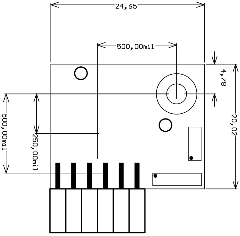
Figure 34: Board physical dimensions drawing.
...
Date | Revision | Contributors | Description | ||||||||
|---|---|---|---|---|---|---|---|---|---|---|---|
| John Hartfiel |
| |||||||||
| 2017-10-19 | v.9 | Ali Naseri |
|
Table 7: Document change history.
...
Overview
Content Tools