Page History
...
- SFP+ connector (Enhanced small form-factor pluggable), supports data transmission rates up to 10 Gbit/s
- Micro-USB-Interface (J10) connected to Zynq-module (Device or OTG mode)
- Trenz 4x5 module Socket (3 x Samtec LSHM series connectors)
- 4x5 SoM programable by JTAG header (JX1)
- 2 x user LEDs routed to IO-pins of the SoM
- Soldering-pads J17 and J20 for optional pin headers for access to SoM's IO-bank-pins, usable as LVDS-pairs
- Soldering-pads J3 and J4 for optional pin headers for access to further interfaces and IO's of the SoM
Block Diagram
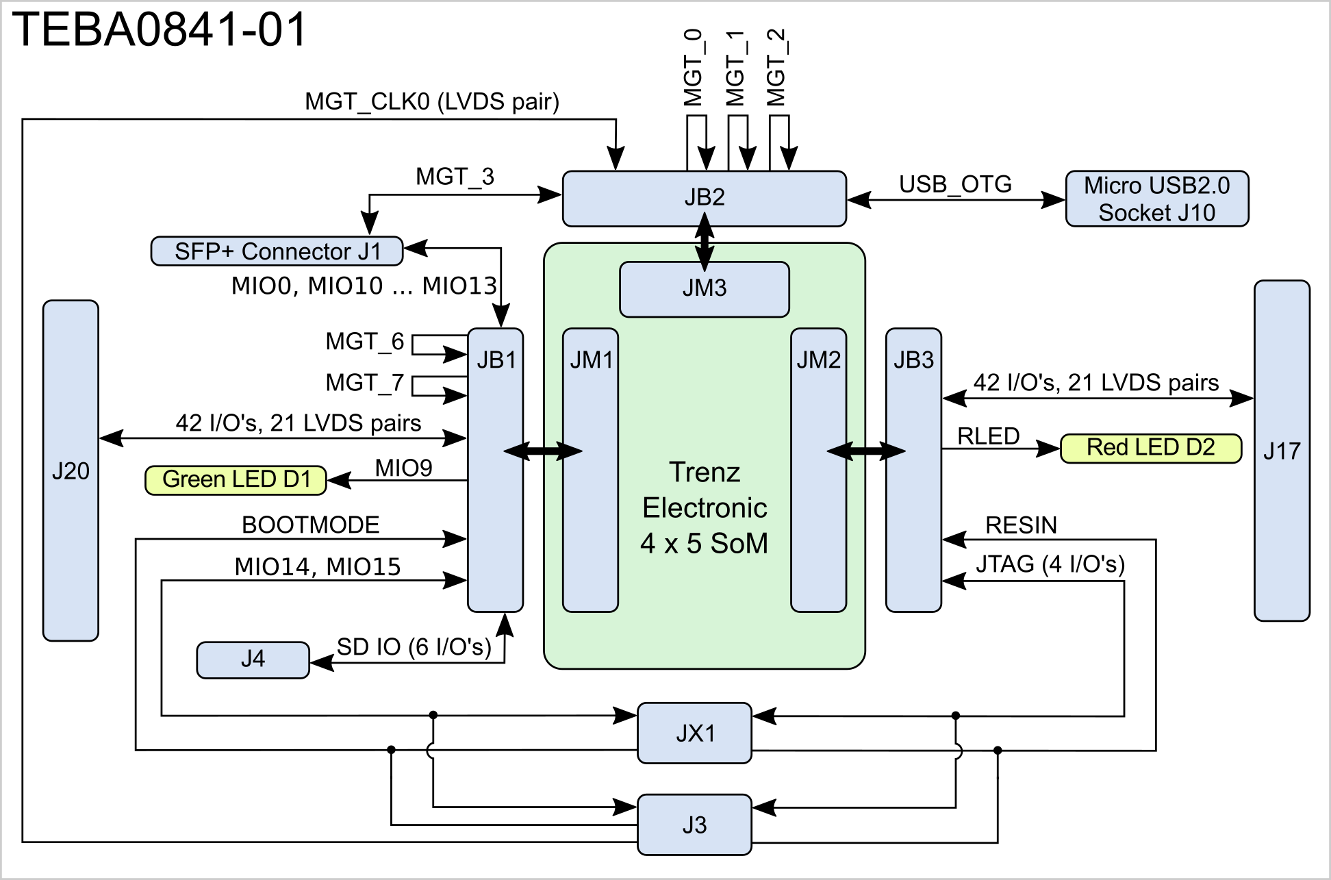
Figure 1: TEBA0841-01 Block Diagram
...
Following table describes how to configure the base-board supply-voltages by jumpers:
Base-board Supply Voltages | VCCIOA | VCCIOD |
|---|---|---|
| 1.8V | J26:1-2 | J27:1-2 |
| 2.5V | J26:3-4 | J27:3-4 |
| 3.3V | J26:5-6 | J27:5-6 |
Table 6: Configuration of base-board supply-voltages via jumpers. Jumper-Notification: 'Jx: 1-2' means pins 1 and 2 are connected, 'Jx: 3-4' means pins 3 and 4 are connected, and so on.
| Note |
|---|
Take care of the VCCO voltage ranges of the particular PL IO-banks (HR, HP) of the mounted SoM, otherwise damages may occur to the FPGA. Therefore, refer to the TRM of the mounted SoM to get the specific information of the voltage ranges. It is recommended to set and measure the PL IO-bank supply-voltages before mounting of TE 4 x 5 module to avoid failures and damages to the functionality of the mounted SoM. |
Technical Specifications
Absolute Maximum Ratings
...
Overview
Content Tools