Page History
...
Control Board Connections
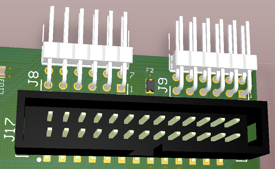
| Signal names | Connector J8 | Connector J9 | Connector J17 |
|---|---|---|---|
Digital Supply to EDPS | Pin 6, 12: +3.3V | Pin 6, 12: +3.3V Pin 5, 11: GND | Pin 5, 6, 21, 22: +3.3V Pin 1, 2, 25, 26: GND |
Motor Driver PWM Signals to EDPS High and Low Side control signals
| Pin 1: G1H - Ch.A HighSide | Pin 11: G1H - Ch.A HighSide | |
| ADC Clock Signal to EDPS | Pin 1: SCLK | Pin 23: SCLK | |
| Encoder Digital Signals from EDPS | Pin 8: ENC_A | Pin 20: ENC_A | |
| Motor Current ADC "raw" Signals from EDPS (usable with FPGA IP) | Pin 2: SDI1 - Current Ch.A | Pin 19: SDI1 - Current Ch.A | |
| Supply Voltage ADC "raw" Signal from EDPS (usable with FPGA IP) | Pin 7: SDIV - from DC_LINK | Pin 24: SDIV - from DC_LINK | |
| 1-Wire bus for temperature measurement | Pin 10: EXT1 - 1-Wire Bus 1 Pin 4: EXT2 - 1-Wire Bus 2 | Pin 4: EXT1 - 1-Wire Bus 1 | |
| Not connected pins | none | none | Pin 13, 14 |
Motor and Power Connections
There are two options available for the motor and power concept:
| Detail | Option 1: Reference Motor Board with DC +12V Supply | Option 2: Customer Motor at individual DC +5..48V | Comments |
|---|---|---|---|
| Motor Supply | From DC +12V Input J7 via Fuse F3 (TODO ... A) | From customer DC Supply to J6 via F1 on Eval Boad | |
| Motor Connection | Motor wires connected to cage clamps on Motor Reference Board J5 (A), J4 (B), J3 (C) | Motor wires connected to bolt screw terminals on Eval Board J2 (A), J3 (B), J4 (C) | |
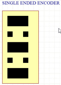
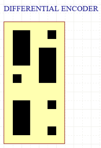
| Encoder Connection | From encoder pins via ribbon cable to Eval Board J10, 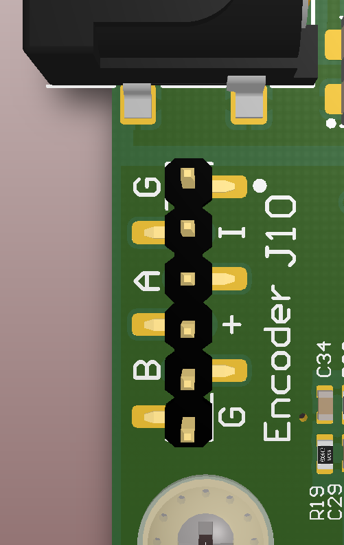 J11 single ended: | From motor to Eval Board J10 (only single ende signals) see left colomn, or to J11 (single OR differential signals): 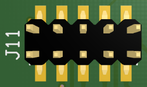 J11 single ended: J11 differential with 100R terminated: | Jumper Settings for encoder signals.
|
Internal
Temperature Sensor
...
- Disconnect the reference motor board TEC0060 by unmounting its screws and the encoder cable from J10
- Mount the delivered 30A fuse to the connectors J5 and J6 with the delivered M5 screws
- For lower supply current requirements, caused by the power rating of the used motor, a fuse with a lower and suitable current rating integrated in the supply wiring is recommended.
- Connect with cable lugs the +DC 5..48V to J6 and the corresponding GND to J1.
- The cable length is limited to 3m.
- Connect the three motor phases to J2 (A), J3 (B) and J4 (C).
- The cable length is limited to 3m.
- Optional: connect the encoder to J10 or J11 and set jumper field according to signal specification: differential or single ended. See section TODO for details.
Power Consumption
Test Condition:
| VIN Current mA | Notes |
|---|---|---|
| TEC0053-03 +3V3 | TODO mA | |
| TEC0053-03 +12V | TODO mA |
Power-On Sequence
Any power sequence of the three supply sources is allowed:
...
Absolute Maximum Ratings - TODO
| Parameter | Min | Max | Units | Notes | Reference document |
|---|---|---|---|---|---|
DC +12V supply | TODO | TODO | V | ||
| DC +5..48V supply | 5 | 48 | V | ||
| DC +3V3 supply | TODO | TODO | V | ||
| PWM Input Logic High Level | TODO | TODO | V | ||
| PWM Input Logic Low Level | TODO | TODO | V | ||
| ADC Digital Output Logic High Level | TODO | TODO | V | ||
| ADC Digital Output Logic Low Level | TODO | TODO | V | ||
| Encoder Input Logic High Level (Differential) | TODO | TODO | V | ||
| Encoder Input Logic Low Level (Differential) | TODO | TODO | V | ||
| Encoder Input Logic High Level ( |
| Single Ended) | TODO | TODO | V | ||
| Encoder Input Logic Low Level ( |
| Single Ended) | TODO | TODO | V |
Recommended Operating Conditions - TOD
| Parameter | Min | Max | Units | Notes | Reference document |
|---|---|---|---|---|---|
DC +12V supply | 11.5 | 12.5 | V | ||
| DC +5..48V supply | 5 | 48 | V | ||
| DC +3V3 supply | TODO | TODO | V | ||
| PWM Input Logic High Level | TODO | TODO | V | ||
| PWM Input Logic Low Level | TODO | TODO | V | ||
| ADC Digital Output Logic High Level | TODO | TODO | V | ||
| ADC Digital Output Logic Low Level | TODO | TODO | V | ||
| Encoder Input Logic High Level (Differential) | TODO | TODO | V | ||
| Encoder Input Logic Low Level (Differential) | TODO | TODO | V | ||
| Encoder Input Logic High Level ( |
| Single Ended) | TODO | TODO | V | ||
| Encoder Input Logic Low Level ( |
| Single Ended) | TODO | TODO | V |
Physical Dimensions
Board size: 100 mm × 166 mm. Please download the assembly diagram for exact numbers.
PCB thickness: 1.75 mm +/-10%
Highest part on PCB: approximately 17 mm. Please download the step model for exact numbers.
...
Operating Temperature Ranges - TODO
Weight - TODO
| Variant | Weight in g | Note |
|---|---|---|
| - | TODO |
|
Revision History
Hardware Revision History - TODO
| Date | Revision | Notes | PCN Link | Documentation Link |
|---|---|---|---|---|
| 2016-03-27 | 02 | TEC0053-02 | ||
| 2017-08-14 | 04 |
Hardware revision number is printed on the PCB board in the down right corner.
Document Change History - TODO
Date | Revision | Authors | Description |
|---|---|---|---|
| 2017-03-30 |
| Andreas Heidemann | Initial Version |
Overview
Content Tools